Argonne National Laboratory Plasma Cleaning Technology
US Patent No 5,510,624issued April 23, 1996
Technique for Simultaneous Specimen & Stage Cleaning for Analytical Electron Microscopy
To download a copy of the Patent in Adobe PDF format click here.
Introduction
A new technique has been developed which allows simultaneous cleaning of a sample and a specimen stage or the internal components of a microscope (polepieces, apertures etc..) which minimizes and, in some cases eliminates, contamination of inorganic specimens analyzed via SEM, TEM, STEM and/or AEM. The technology involves subjecting the specimen and the specimen stage to a reactive plasma gas (either DC or RF excited) which efficiently removes a wide range of contaminants from critical surfaces. The procedure may be carried out prior to inserting the specimen and specimen stage into the EM by either mounting the specimen holder in the supplied put or by inserting the entire sample or sample assembly into a plasma reaction chamber. The system can be used with any side entry TEM holders, top entry TEM holders or with any sample that will fit inside the large, easily accessible chamber.
Background
Microcharacterization of materials by electron microscopy is ultimately limited by the ability to observe, detect and analyze the constituent materials present in micro volumes of specimen in the environment of the electron microscope, the interaction of surface borne contaminants with the high energy incident electron probe can create deposits on the surfaces of a sample which can prohibit these analyses These contaminants may be introduced directly by the specimen, deposited on the specimen via the specimen stage or deposited on the specimen via the microscope system. Electron microscope manufacturers attempt to minimize the last of these by judicious design. However, the first two sources of contaminant introduction are out of their direct control.
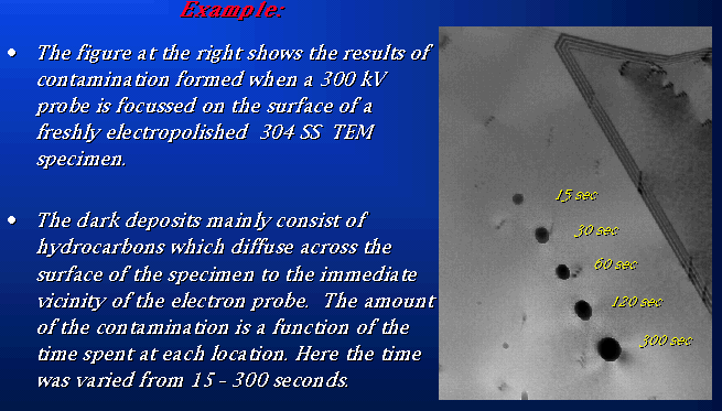
Surface borne contamination is introduced in the preparation of inorganic specimens (metals, ceramics, semiconductors etc.) for EM work. The materials to be studied are frequently subjected to chemical or electrochemical polishing followed by solvent rinsing and air drying. This typically leaves residual organic material on the specimen surface Attempts to clean the specimen stage include rinsing the stage with various solvents. Improper or poor techniques used to store both specimens and/or stages prior to insertion in the microscope can introduce additional organic residue. Finally, contamination derived within in the instrument can mitigate analysis. While the majority of the organics involved m these processes dissipate, a small amount generally remains on the surfaces and is sufficient to cause problems when the specimen is subsequently examined in modern analytical microscopes. Although these organic residues are widely distributed and generally at low concentrations on the various surfaces, they can become mobile in the microscope environment and are attracted to the periphery of any focused electron probe, forming deposits (figure 1). Since these contaminants can travel large distances over the surface of the specimen, it is important to remove or immobilize them as much as prior an analysis without disturbing the microstructure of the specimen. It is important to note that once the deposits are formed, they are not easily removed. Analysis of a "corrupted" area is precluded
Procedure
It has been well documented that low temperature plasmas can be used to reactively etch ash organic materials found on the surface of inorganic materials. This has been used by the Industrial community to clean semi-conductor wafers and other bulk materials for many years. In this procedure, a related technique is employed for the cleaning of EM specimens. Instead of subjecting only the material of interest (i e. specimen) to the plasma, the entire stage and sample is plasma cleaned (figure 2) The nature of the gas selected is based upon the desired effect Although an argon - oxygen mix is generally used, specific gases ( BCl3, CF4, .. .) may be used to tailor a reaction. Cleaning time is typically 10-30 minutes. Specimens that previously contaminated m minutes can after treatment, be studied for several hours (Fig. 3 & 4).
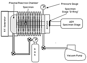
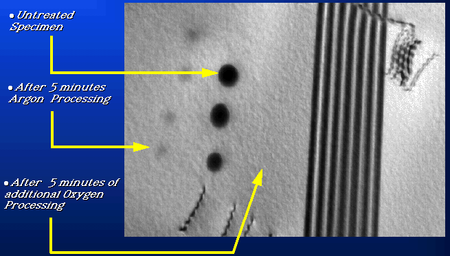
Figure 3. Illustration of contamination and it's elimination using the ANL Technology. Large dark marks caused by focussed electron probe on a virgin sample, followed by 5 Minutes of treatment using an Argon plasma, followed by 5 Mintues of treatment with an Oxygen plasma
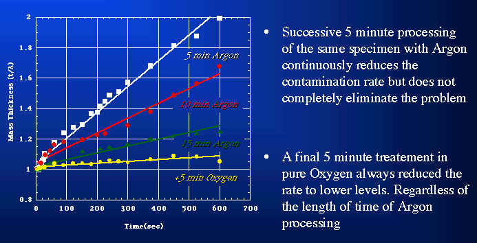
Figure 4. Quantitative Measurements in the reduction of contamination as a function of plasma processing time and gas composition.
To obtain additional detailed information about the process you can download a copy of the ANL Patent, an article from Microscopy & Microanalysis-97 Meeting or a poster from Materials Research Society Spring-97 Meeting, or the following Book Chapter PlasmaCleaningPaperFinal.pdf. All these documents are stored in Adobe Acrobat Format on the ANL WWW site. You may download a FREE Adobe Reader/Viewer to be able to read these documents on Mac, Windows, or Unix Platforms.
The following Commerical Organizations have Licensed this Technology from ANL and produce a product which implements this procedure in TEM's or SEM's
Additional information about licensing of the ANL Technology can be obtained by calling the Technology Transfer Office at 630-252-9771.