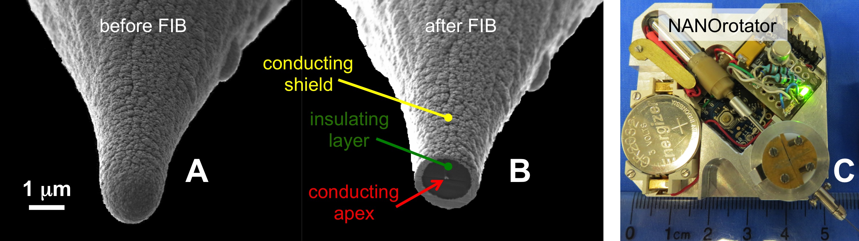
| The insulating layer of smart tips can reduce the detection of photoejected electrons from the sample at the sidewalls of the tip. However, charging of the insulator with photoejected electrons can occur and interfere with the tunneling process. To overcome this hurdle, we have recently developed a novel type of smart STM tips (United States Patent 8,850,611). These are nanofabricated coaxial metal-insulator-metal (MIM)-tips with an outer conducting shell covering the insulating layer. |
|
|
| After coating a sharp metallic tip, the tip apex is exposed by removing the coated films using focused ion beam (FIB) milling. For this purpose, a specialized programmable nanoROTATOR was designed to provide an additional degree of freedom, allowing the tip to spin around its axis during FIB milling. The resulting smart tips are ultra sharp with typically only around 20-30 nm of the apex exposed. The outermost conducting layer of the tip can be biased or grounded independently from the tunneling bias of the STM. |
|
|
| Previous | Back to Research |