|
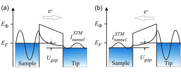
The scanning tunneling microscope (STM) is based on a quantum mechanical effect. When a sharp conducting tip is brought close to a conductive sample, a bias voltage can allow electrons to tunnel through the vacuum gap between them. The applied bias voltage between the tip and the sample determines the direction of the electron tunneling. When the sample is negatively biased (left), electrons tunnel from the occupied states of the sample into the unoccupied states of the tip. In the case of a positively biased sample (right), electrons tunnel from the occupied states of the tip to the unoccupied states of the sample. Only electrons close to the Fermi energy EF contribute to the tunneling current. Unfortunately, these electrons do not carry any direct chemical information about their originating atoms.
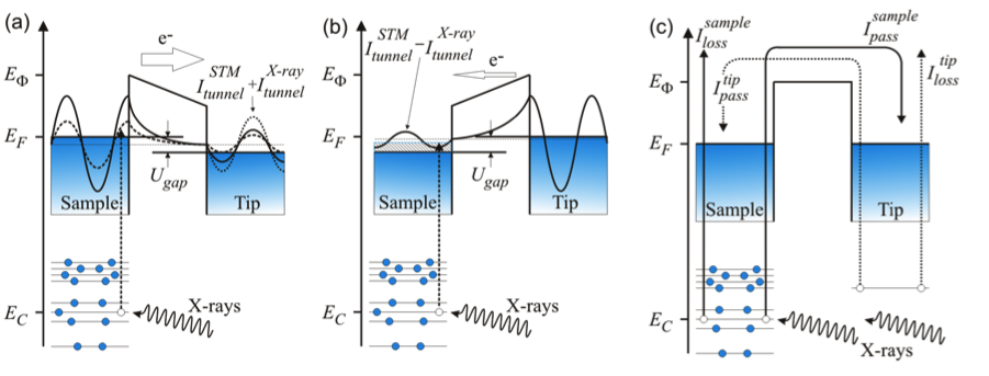
In spite of the very high spatial resolution, conventional STM does not provide direct chemical information about sample surfaces. However, if a sample is illuminated with monochromatic x-rays, characteristic absorption will arise. When the excitation energy is tuned to a core level energy EC, a jump-wise increase in the number of excited electrons occurs, and core electrons are excited into unoccupied states above the Fermi level EF. Depending on the sign of the applied bias between the tip and the sample, those excited electrons might increase (left) or decrease (center) the conventional tunnel current. Electrons with energy greater than the work function can escape from the sample and generate a photocurrent (right), which has to be controlled by smart tips. These ejected electrons can be exploited for the combination of atomic force microscopy (AFM) and x-rays. After electrons are ejected from either the sample or the tip they are accelerated in the electric field generated by the bias voltage between tip and sample. In particular, secondary electron emission is dominated by low-energy electrons, which are extremely sensitive to an electric field. If the sample is positively biased, photoelectrons are prone to be recollected by the sample, while the tip repels those photoelectrons due to the relatively negative potential. The situation is reversed when the sample is negatively biased. Thus, the sign and the size of the bias voltage allow for controlling the photoelectron channel while the AFM will image the topography of the sample surface.
|