Scientific Achievement
The use of focused ion beam (FIB) technology at the Electron Microscopy Center has been the key enabler for the development of a novel x-ray microscopy technique at the Advanced Photon Source. The high resolution imaging capability at the EMC coupled with the in situ nanofabrication faculties have enabled us to develop new kinds of sharp probes that are entirely coated by an insulating film except at the very tip apex. These “smart tips” serve as nanoscale detectors.
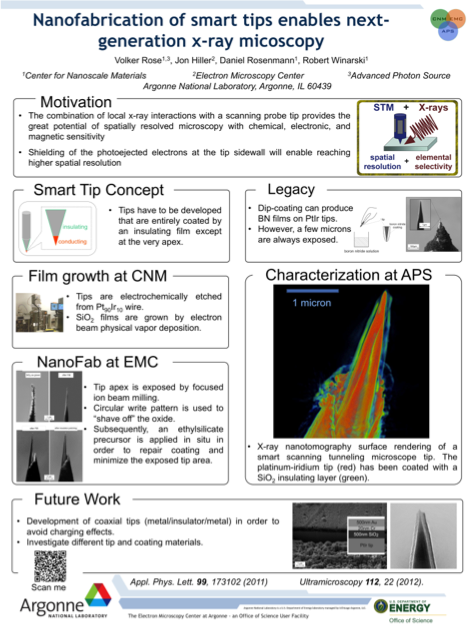
Insulating SiO2 films have been removed from the apex of platinum-iridium scanning probe tips by means of high-resolution focused ion beam milling using a shadow masking technique. After coating of sharp PtIr tips with an insulating film by electron beam physical vapor deposition, we have used FIB to fabricate tips with sub-100-nm exposed conducting apex. This achievement is an important cornerstone for the development of a next-generation x-ray microscope.
Significance
Synchrotron x-ray scanning tunneling microscopy (SX-STM) is a promising new x-ray microscopy technique that has the potential to provide direct chemical contrast at the nanoscale. This technique combines the high spatial resolution of STM with the electronic, chemical, and magnetic sensitivity of synchrotron x-rays. While a sharp tip is rastering across a surface, absorption of photons by the sample can excite electrons to unoccupied levels close to Fermi energy. At the same time photoelectrons are ejected from the sample. The conducting tip that is tunneling over a sample surface can locally measure these excited electrons. However, photoejected electrons will also be detected at the sidewall of the tip, which will drastically limit the achievable spatial resolution. This problem has been solved by specialized insulator coated tips with minimized conducting apex, which reduce the detection of photoejected electrons at the sidewall. This work has been published in Appl. Phys. Lett. 99, 173102 (2011).
|