
Wide bandgap (WBG) semiconductors are essential to our technology future [1]. Power electronics made with WBG components overcome the upper limits on temperature, frequency, and voltage that apply to silicon based electronics and can help to eliminate up to 90% of present-day power losses in electric conversion. They are foreseen as essential for future development of electric vehicles, industrial motors, laptop power converters and inverters for connecting wind turbines, and solar panels to the power grid [1]. A wide bandgap also makes them ideal for ultraviolet (UV) detectors that must be blinded from visible light in the solar spectrum, so-called "solar-blind detectors". Another application is to UV laser diodes. These applications, in general, require single-crystal material, and device performances are degraded by crystalline defects such as dislocations. Dislocations are also deleterious for reliability and lifetimes of devices. X-ray topography is a potent and non-invasive technique for imaging dislocation arrays in crystals, and work to characterize dislocation arrays in aluminum nitride, a WBG semiconductor, by means of x-ray topography has been carried out at the APS by researchers from Stony Brook University. Their work was published in a recent paper [2].
The wurtzite III-V nitride binary compounds of indium nitride (InN), gallium nitride (GaN), and aluminum nitride (AlN) have bandgaps of 1.9 eV, 3.4 eV, and 6.2 eV, respectively. They form a continuous range of compounds useful for optoelectronic sources and detectors at UV wavelengths, much like the III-V arsenides and III-V phosphides are useful at visible and infrared wavelengths [3]. Heteroepitaxy is a widely applied technology for device fabrication, but because lattice parameters do not match those of readily available substrates (e.g., sapphire), mismatch dislocations in epitaxial layers occur. Consequently, single-crystal boules of III-V nitrides are much desired to provide substrate wafers, and crystal growth of III-V nitride boules is an important technological effort. The melting temperature of InN, GaN, and AlN also follows an upward progression, with a melting temperature of AlN in excess of 3000° C. Such a high melting point is problematic for crystal growth from the melt [4]. This dilemma is finessed by the technique of physical vapor transport (PVT). For PVT, powdered AlN is sublimed in one chamber and transported with gaseous N2 to a second chamber that is held at a temperature that is approximately 1000° C lower [4]. The AlN studied at APS beamline 1-BM was grown by PVT from an AlN seed placed in the growth chamber.
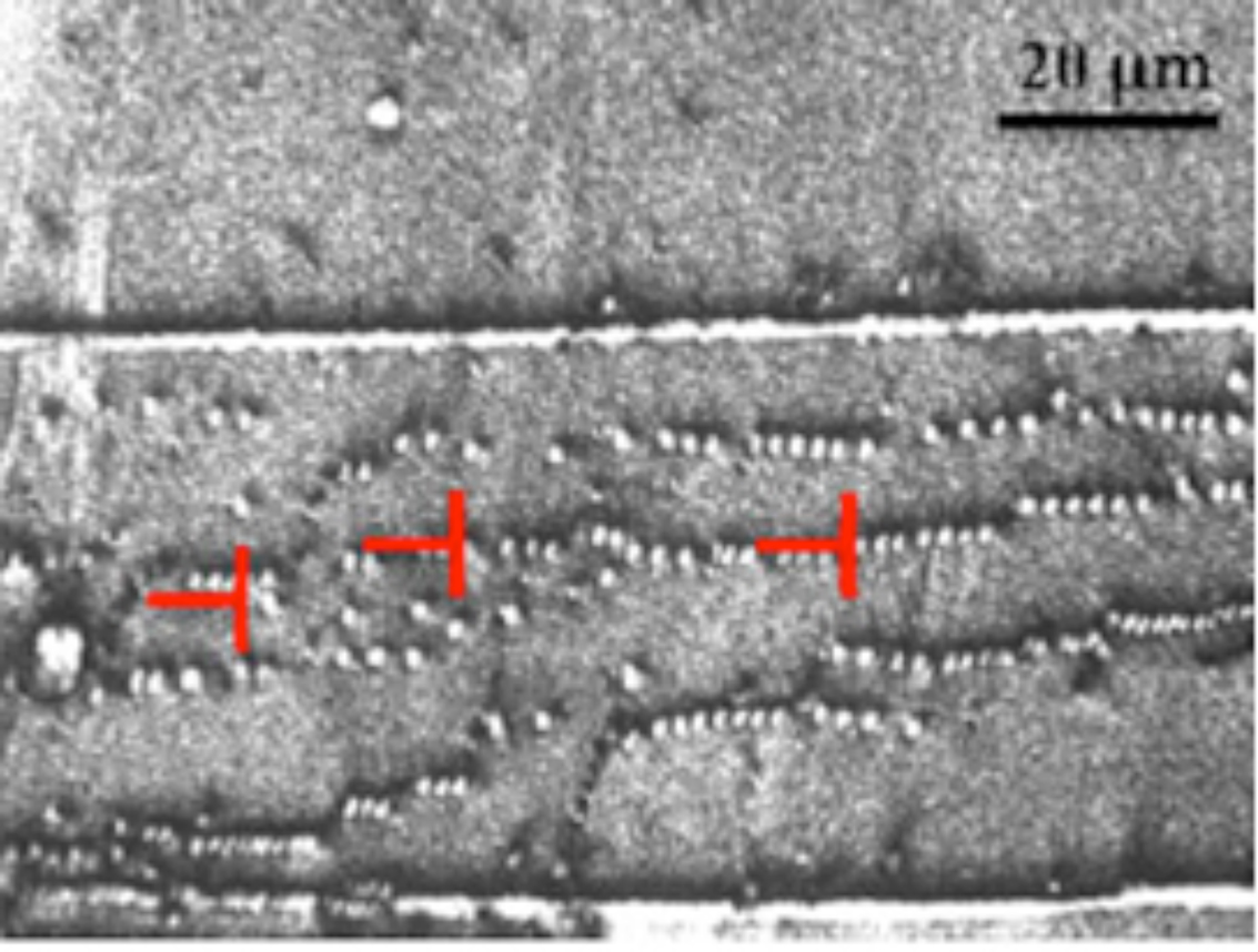
A remaining technological emphasis is to grow crystals with very low dislocation densities. Dislocation densities need to be low so that devices fabricated on wafers cut from boules achieve an optimum performance. A readily applied method to characterize threading dislocations is to etch the surface to reveal etch pits. But one cannot determine the orientation of the displacement vector that characterizes the dislocation this way [2]. The displacement vector of a dislocation is determined by schematically making an atom-to-atom circuit around a region of crystal that contains the dislocation. Without the dislocation this circuit would be closed, but because of the dislocation there is a displacement vector between start and end. This is the displacement vector that characterizes the dislocation. However, a novel technique was able to determine the entire displacement vector for threading dislocations [2]. This technique combines grazing incidence x-ray topography with ray tracing simulations. Dislocations thread along the c-axis of the wurtzite crystal structure. There are six possible types of threading edge dislocations (TEDs) and two possible types of threading screw dislocations (TSDs). With grazing incidence x-ray topography, accompanied by ray tracing simulations, for the first time it was possible to sort out which of these possible dislocations were prevalent in the PVT-grown material [2]. TEDs were found to occur in arrays of two kinds: 1) oriented along <1 -1 0 0>, and 2) oriented along <1 1 -2 0>. The most prevalent was type 1). This characterization of the line defects occurring in PVT-grown AlN provides a bench mark against which future improvements in crystal quality can be judged. Contact: Al Macrander, [email protected]
References
[1] http://energy.gov/articles/wide-bandgap-semiconductors-essential-our-te…
[2] T. Zhou, B. Raghothamachar, F. Wu, R. Dalmau, B. Moody, S. Craft, R. Schlesser, M. Dudley, and Z. Sitar, J. Electronic Materials, DOI:10.1007/s11664-013-2968-2 (2014).
[3] S. Strite and H. Morkoc, J. Vac. Sci. Tech. B 10, 1237 (1992).
[4] G. Dhanaraj, K. Byrappa, V. Prasad, and M. Dudley, "Handbook of Crystal Growth", Springer, 2010.
Financial support from DARPA via HexaTech, Inc. Monochromatic x-ray topography was carried out at the 33-BM-C and 1-BM-B,C beamlines of the APS, which is supported by the U.S. Department of Energy (DOE) Office of Science under Contract No. DE-AC02-06CH11357. The published work was in part also based on white-beam x-ray topography carried out at the Stony Brook Topography Facility (Beamline X19C) at the National Synchrotron Light Source, Brookhaven National Laboratory, supported by the DOE under Contract No. DE-AC02-76CH00016.
The Advanced Photon Source at Argonne National Laboratory is one of five national synchrotron radiation light sources supported by the U.S. Department of Energy's Office of Science to carry out applied and basic research to understand, predict, and ultimately control matter and energy at the electronic, atomic, and molecular levels, provide the foundations for new energy technologies, and support DOE missions in energy, environment, and national security. To learn more about the Office of Science x-ray user facilities, visit http://science.energy.gov/user-facilities/basic-energy-sciences/.
Argonne National Laboratory seeks solutions to pressing national problems in science and technology. The nation's first national laboratory, Argonne conducts leading-edge basic and applied scientific research in virtually every scientific discipline. Argonne researchers work closely with researchers from hundreds of companies, universities, and federal, state and municipal agencies to help them solve their specific problems, advance America's scientific leadership and prepare the nation for a better future. With employees from more than 60 nations, Argonne is managed by UChicago Argonne, LLC for the U.S. Department of Energy's Office of Science.