
The original Penn State University press release by Walt Mills can be read here.
A team of materials scientists carrying out research at the U,.S. Department of Energy’s Advanced Photon Source (APS) have, for the first time, visualized the three-dimensional atomic and electron density profile of the most complex perovskite crystal structure system decoded to date.
Perovskites are minerals that are of interest as electrical insulators, semiconductors, metals or superconductors, depending on the arrangement of their atoms and electrons.
Perovskite crystals have an unusual grouping of oxygen atoms that form an octahedron — an eight-sided polygon. This arrangement of oxygen atoms acts like a cage that can hold a large number of the elemental atoms in the periodic table. Additionally, other atoms can be fixed to the corners of a cube outside of the cage at precise locations to alter the material’s properties, for instance in changing a metal into an insulator, or a non-magnet into a ferromagnet.
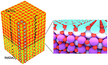
In their current work, the team from Penn State University, Cornell University, and Argonne National Laboratory grew the very first discovered perovskite crystal, called calcium titanate, on top of a series of other perovskite crystal substrates with similar but slightly different oxygen cages at their surfaces. Because the thin-film perovskite on top wants to conform to the structure of the thicker substrate, it contorts its cages in a process known as “tilt epitaxy.” The researchers found that this tilt epitaxy of calcium titanate caused a very ordinary material to become ferroelectric — a spontaneous polarization — and to remain ferroelectric up to 900 Kelvin, around three times hotter than room temperature. They were also able to visualize the three-dimensional electron density distribution in calcium titanate thin film for the first time.
“We have been able to see atoms for quite some time, but not map them and their electron density distribution in space in a crystal in three dimensions,” said Venkat Gopalan, professor of materials science and physics, Penn State. “If we can see not just where atomic nuclei are located in space, but also how their electron clouds are shared, that will tell us basically everything we need to know about the material in order to infer its properties.”
That was the challenge the team set for itself over five years ago when Gopalan gave the project to his student and lead author of a new report in Nature Communications, Yakun Yuan. Based on a rarely used x-ray visualization technique called COBRA, (coherent Bragg rod analysis) originally developed by a group in Israel, Yuan figured out how to expand and modify the technique to analyze one of the most complicated, least symmetrical material systems studied to date. This system is a strained three-dimensional perovskite crystal with octahedral tilts in all directions, grown on another equally complex crystal structure.
“To reveal three-dimensional structural details at the atomic level, we had to collect extensive datasets … and carefully analyze them with the COBRA analysis code modified for accommodating the complexity of such low symmetry,” said Yuan. In collaboration with APS beamline scientist Dr. Hua Zhou, the surface x-ray diffraction data sets were obtained utilizing high-brightness x-ray beams from the X-ray Science Division 12-ID-D and 33-ID-D beamlines at the Advanced Photon Source, an Office of Science user facility at Argonne.
Gopalan went on to explain that very few perovskite oxygen cages are perfectly aligned throughout the material. Some rotate counterclockwise in one layer of atoms and clockwise in the next. Some cages are squeezed out of shape or tilt in directions that are in or out of plane to the substrate surface. From the interface of a film with the substrate it is grown on, all the way to its surface, each atomic layer may have unique changes in their structure and pattern. All of these distortions make a difference in the material properties, which they can predict using a computational technique called density functional theory (DFT).
“The predictions from the DFT calculations provide insights that complement the experimental data and help explain the way that material properties change with the alignment or tilting of the perovskite oxygen cages,” said Susan Sinnott, professor of Materials Science and Engineering at Penn State, whose group performed the theoretical calculations.
The team also validated their advanced COBRA technique against multiple images of their material using the powerful Titan transmission electron microscope in the Materials Research Institute at Penn State. Since the electron microscopes image extremely thin electron transparent samples in a two-dimensional projection, not all of the three-dimensional image could be captured even with the best microscope available today and with multiple sample orientations. This is an area where three-dimensional dimensional imaging by synchrotron x-rays and the COBRA technique outperformed the electron microscopy in imaging such complex structures.
The researchers believe their COBRA technique is applicable to the study of many other three-dimensional, low-symmetry atomic crystals.
See: Yakun Yuan1, Yanfu Lu1, Greg Stone1, Ke Wang1, Charles M. Brooks2, Darrell G. Schlom2,3, Susan B. Sinnott1, Hua Zhou4*, and Venkatraman Gopalan1**, “Three-dimensional atomic scale electron density reconstruction of octahedral tilt epitaxy in functional perovskites,” Nat. Commun. 9, 5220 (2018). DOI: 10.1038/s41467-018-07665-1
Author affiliations: 1Pennsylvania State University, 2Cornell University, 3Kavli Institute at Cornell for Nanoscale Science, 4Argonne National Laboratory
Correspondence: * [email protected], ** [email protected]
This work was supported by the U.S. National Science Foundation (NSF) MRSEC Center for Nanoscale Science under award no. DMR-1420620. The DFT study is conducted as part of The Pennsylvania State University (PSU) 2D Crystal Consortium – Materials Innovation Platform under NSF award No. DMR-1539916. Support was also received from the PSU’s Institute for CyberScience through a Graduate Research Assistantship. We thank Zhan Zhang for the help with synchrotron x-ray diffraction at 33-ID-D, and Haiying Wang from the Materials Characterization Laboratory at Penn State for the help with STEM sample preparation. This research used resources of the Advanced Photon Source, a U.S. Department of Energy (DOE) Office of Science User Facility operated by Argonne National Laboratory under Contract No. DE-AC02- 06CH11357.
Argonne National Laboratory seeks solutions to pressing national problems in science and technology. The nation's first national laboratory, Argonne conducts leading-edge basic and applied scientific research in virtually every scientific discipline. Argonne researchers work closely with researchers from hundreds of companies, universities, and federal, state and municipal agencies to help them solve their specific problems, advance America's scientific leadership and prepare the nation for a better future. With employees from more than 60 nations, Argonne is managed by UChicago Argonne, LLC for the U.S. Department of Energy's Office of Science.
The U.S. Department of Energy's Office of Science is the single largest supporter of basic research in the physical sciences in the United States and is working to address some of the most pressing challenges of our time. For more information, visit the Office of Science website.