
The original University of Illinois at Chicago press release by Sharon Parmet can be read here.
Researchers utilizing intense x-ray beams from the U.S. Department of Energy’s Advanced Photon Source (APS) examined the flow of electricity through semiconductors and uncovered another reason these materials seem to lose their ability to carry a charge as they become more densely “doped.” Their results, which may help engineers design faster semiconductors in the future, were published online in the journal ACS Nano.
Semiconductors are found in just about every piece of modern electronics, from computers to televisions to your cell phone. They fall somewhere between metals, which conduct electricity very well, and insulators like glass that don’t conduct electricity at all. This moderate conduction property is what allows semiconductors to perform as switches and transistors in electronics.
The most common material for semiconductors is silicon, which is mined from the Earth and then refined and purified. But pure silicon doesn’t conduct electricity, so the material is purposely and precisely adulterated by the addition of other substances known as dopants. Boron and phosphorus ions are common dopants added (doped) to silicon-based semiconductors that allow them to conduct electricity.
But the amount of dopant added to a semiconductor matters – too little dopant and the semiconductor won’t be able to conduct electricity; too much dopant and the semiconductor becomes more like a non-conductive insulator.
“There’s a sweet spot when it comes to doping where the right amount allows for the efficient conduction of electricity, but after a certain point, adding more dopants slows down the flow,” says Preston Snee, associate professor of chemistry at the University of Illinois at Chicago (UIC) and corresponding author on the paper.
“For a long time scientists thought that the reason efficient conduction of electricity dropped off with the addition of more dopants was because these dopants caused the flowing electrons to be deflected away, but we found that there’s also another way too many dopants impede the flow of electricity.”
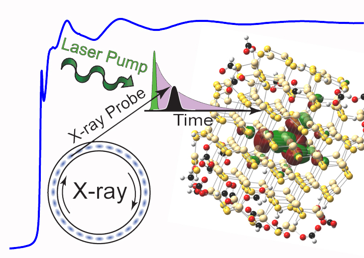
Snee, UIC chemistry student Asra Hassan, and their colleagues from UIC, Northwestern University, and Argonne National Laboratory wanted to get a closer look at what happens when electricity flows through a semiconductor.
To do that, the team employed a variety of synchrotron techniques at several APS x-ray beamlines. Static copper K-edge XANES measurements were performed at the Materials Research Collaborative Access Team (MR-CAT) 10-ID-B x-ray beamline. Additional static and ultrafast time-resolved x-ray absorption experiments were carried out at the X-ray Science Division (XSD) 11-ID-D x-ray beamline, and small-angle x-ray scattering analysis was done at the XSD beamline 12-ID-B. (The APS is an Office of Science user facility at Argonne.)
These studies elucidate what happens at the atomic level inside a semiconductor. The research team used tiny chips of cadmium sulfide for their semiconductor “base” and doped them with copper ions. Instead of wiring the tiny chips for electricity, they generated a flow of electrons through the semiconductors by shooting them with a powerful blue laser beam. At the same time, they captured very-high-energy x-ray images of the semiconductors at millionths of a microsecond apart – which showed what was happening at the atomic level in real time as electrons flowed through the doped semiconductors.
They found that when electrons were flowing through, the copper ions transiently formed bonds with the cadmium sulfate semiconductor base, which is detrimental to conduction.
“This has never been seen before,” said Hassan. “Electrons are still bouncing off dopants, which we knew already, but we now know of this other process that contributes to impeding flow of electricity in over-doped semiconductors.”
The bonding of the dopant ions to the semiconductor base material “causes the current to get stuck at the dopants, which we don’t want in our electronics, especially if we want them to be fast and efficient,” she said. “However, now that we know this is happening inside the material, we can design smarter systems that minimize this effect, which we call ‘charge carrier modulation of dopant bonding’.”
See: Asra Hassan1, Xiaoyi Zhang2, Xiaohan Liu1, Clare E. Rowland3, Ali M. Jawaid1, Soma Chattopadhyay2, Ahmet Gulec1, Armen Shamirian1, Xiaobing Zuo2, Robert F. Klie1, Richard D. Schaller2,3, and Preston T. Snee1*, “Charge Carriers Modulate the Bonding of Semiconductor Nanoparticle Dopants As Revealed by Time-Resolved X‑ray Spectroscopy,” ACS Nano, Article ASAP, published on-line August 28, 2017. DOI: 10.1021/acsnano.7b04414
Author affiliations: 1University of Illinois at Chicago, 2Argonne National Laboratory, 3Northwestern University
Correspondence: *[email protected]
Startup funding to PTS from the University of Illinois at Chicago supported this work. MR-CAT operations are supported by the Department of Energy and the MRCAT member institutions. This research used resources of the Advanced Photon Source, a U.S. Department of Energy (DOE) Office of Science User Facility operated for the DOE Office of Science by Argonne National Laboratory under Contract No. DE-AC02-06CH11357.
Argonne National Laboratory seeks solutions to pressing national problems in science and technology. The nation's first national laboratory, Argonne conducts leading-edge basic and applied scientific research in virtually every scientific discipline. Argonne researchers work closely with researchers from hundreds of companies, universities, and federal, state and municipal agencies to help them solve their specific problems, advance America's scientific leadership and prepare the nation for a better future. With employees from more than 60 nations, Argonne is managed by UChicago Argonne, LLC for the U.S. Department of Energy's Office of Science.
The U.S. Department of Energy's Office of Science is the single largest supporter of basic research in the physical sciences in the United States and is working to address some of the most pressing challenges of our time. For more information, visit the Office of Science website.