
Engineers designing integrated circuits often intentionally create small distortions of the structure as one way of enhancing the performance of semiconductor devices. Introducing this strain can change the semiconductor’s electronic properties and affect parameters such as the current that can be driven through a field-effect transistor. Having a way to understand and control strain on very tiny scales could help in designing new generations of devices, from better fuel cells to circuits for quantum computers. Sorting out the effects of strains in an region 100 nm or less across, when the structure is expanding or shrinking by only one 100th of 1%, has been extremely challenging. Now a group of researchers has developed techniques that used a tightly focused x-ray beam at the U.S. Department of Energy’s Advanced Photon Source (APS) at Argonne National Laboratory to measure strain in small volumes. The method can be easily adapted to other material systems where there is a need to understand complex diffraction patterns. It could be applied to other semiconductor materials, as well as to complex oxide materials used in building fuel cells, in which strain can affect the catalytic activity of the oxide.
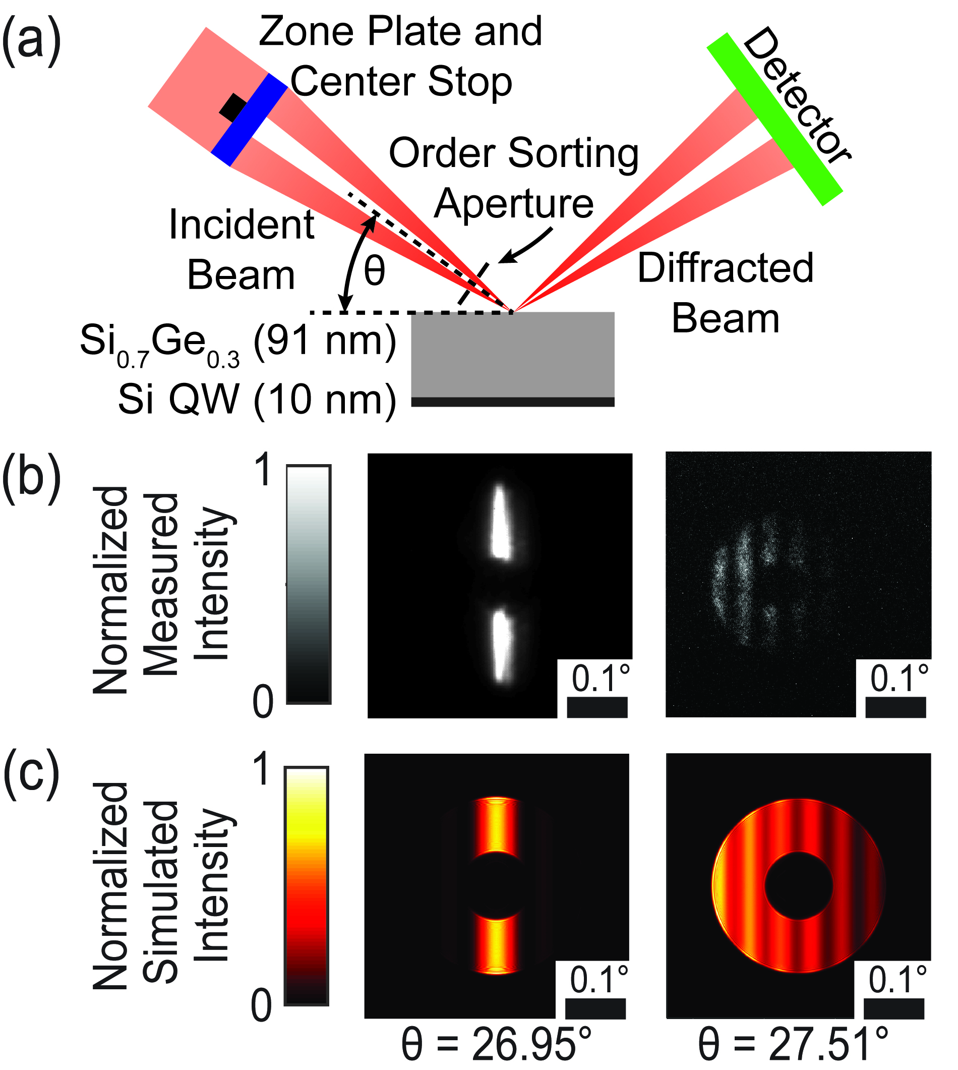
Researchers from the University of Wisconsin-Madison and Argonne studied the x-ray nanobeam diffraction patterns from a semiconductor structure that consisted of a 91-nm-thick layer of silicon-germanium and a 10-nm-thick film of silicon. In x-ray diffraction, an x-ray beam strikes a crystalline structure and produces a pattern, with varying x-ray intensity that depends on the arrangement of atoms within the structure and on the angle at which the beam hits the crystal. Such patterns reveal structural information about the portion of the sample with which the x-rays have interacted. One key advantage of the technique is that the x-rays can measure small strains without preparations that destroy the sample, so the subtle mechanical effects producing the strain are preserved.
The technique gets tricky when it’s applied to strain in a small volume, however. In order to make the measurements on such tiny scales, the beam has to be focused to a very small spot. In this case, the researchers used a Fresnel zone plate to focus the beam to spot sizes approximately 30 to 50 nm across, producing an angular divergence on the order of 100ths of degrees. The Hard X-Ray Nanoprobe at APS beamline 26-ID, operated jointly by the APS and the Center for Nanoscale Materials (CNM) both of which are Office of Science user facilities, provided a narrow beam with a short x-ray wavelength to produce diffraction patterns from the crystal.
Though scientists have developed methods to interpret diffraction patterns, the addition of the focusing optics makes the pattern much more complex. To sort out this problem, the researchers calculated the diffraction patterns that should be produced by layered semiconductor structures. The method involves calculating the wave field of the focused x-ray beam, and of the beam after it is scattered by the sample. Propagating this scattered beam to the location of the detector produces an accurate simulation of the diffraction pattern and the variation of its intensity at different locations on the sample. Features such as interference fringes depend on the angle between the incoming x-ray beam and the sample, and provide information about the mechanical distortion of the lattice. By comparing the simulated diffraction patterns with those produced by their experiment, the researchers could measure these quantities precisely in any spot on the sample and find the mechanical deformation caused by the stress. — Neil Savage
See: J. A. Tilka1, J. Park1, Y. Ahn1, A. Pateras1, K.C. Sampson1, D.E. Savage1, J.R. Prance1, C.B. Simmons1, S.N. Coppersmith1, M.A. Eriksson1, M.G. Lagally1, M.V. Holt2, and P.G. Evans1*, “Combining experiment and optical simulation in coherent X-ray nanobeam characterization of Si/SiGe semiconductor heterostructures,” J. Appl. Phys. 120, 015304 (2016). DOI: 10.1063/1.4955043
Author affiliations: 1University of Wisconsin-Madison, 2Argonne National Laboratory
Correspondence: *[email protected]
J.P., Y.A., A.P., and P.G.E. were supported by the U.S. Department of Energy (DOE) Office of Science-Basic Energy Sciences, Materials Sciences and Engineering, under Contract No. DE-FG02-04ER46147 for the x-ray scattering studies and analysis. J.A.T. acknowledges support from the National Science Foundation (NSF) Graduate Research Fellowship Program under Grant No. DGE-1256259. Development and maintenance of the growth facilities used for fabricating samples are supported by the U.S. DOE (DEFG02- 03ER46028). The other authors acknowledge support from the Army Research Office (W911NF-08-1-0482, W911NF-12-1-0607) and NSF (DMR-1206915). This research used NSF-supported shared facilities supported by the University of Wisconsin Materials Research Science and Engineering Center (DMR- 1121288). Use of the Center for Nanoscale Materials and the Advanced Photon Source, both Office of Science user facilities, was supported by the U.S. DOE Office of Science-Basic Energy Sciences, under Contract No. DE-AC02-06CH11357.