
Quantum computers could vastly outperform today’s most advanced microprocessors in some important computational problems. Instead of switching current flow on and off to create the 1s and 0s of binary code, quantum computers rely on quantum mechanical properties of electrons, such as orbital state and spin. To make this happen, engineers have to develop quantum bits, or qubits, which they can reliably and predictably control; however, this has been a challenging task. Now, a team of researchers using the U.S. Department of Energy’s Advanced Photon Source (APS) and Center for Nanoscale Materials (CNM), Office of Science user facilities at Argonne National Laboratory, have revealed one issue that makes building such qubits so difficult. Armed with this information, the researchers hope engineers will be better able to predict the performance of their devices based on the stress from the electrodes, and perhaps alter their designs to compensate for it. It might even be possible to take advantage of the strain in designing the quantum dots, modifying it to change the electronic properties of the material. Gaining greater control over the electronic properties of the material may also allow researchers to create arrays of qubits with complicated structures to help them better understand the physics of confined electrons.
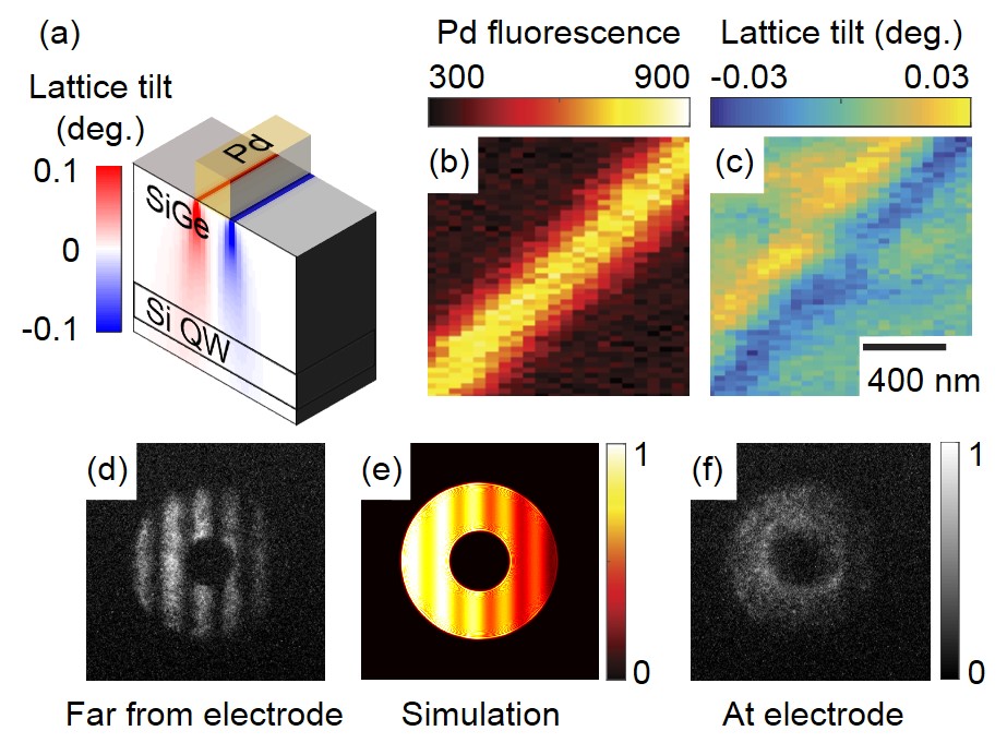
One method for making qubits involves creating quantum dots, which are tiny volumes of a semiconductor that can trap a single electron in a space known as a “quantum well.” Researchers create a device with a thin film of silicon, sandwiched between two thicker films of a silicon-germanium alloy. In the particular structure probed at the joint APS/CNM Hard X-Ray Nanoprobe at APS beamline 26-ID-C, these layers had thicknesses of 10, 91, and 300 nm. The researchers from the University of Wisconsin-Madison and Argonne capped the stack with a thin silicon layer and above it created a pattern of thin-film electrodes made of a metal such as palladium in order to set the location of the quantum well. The electric fields produced by the electrodes pushed electrons away, leaving only small spaces within the quantum well where the electrons could be confined—trapped at the interface between the silicon and the silicon-germanium. These locations are the quantum dots.
Working at such scales, tiny imperfections such as stresses induced by random variations in how the silicon-germanium crystal grows can throw off the properties of the device, making its performance difficult to predict. The variability produces mechanical strain in the devices, which changes how electrons move through the quantum wells. As a result, the engineers cannot tell what voltage will be needed to confine an electron in a given quantum dot, so they try out several until they hit the sweet spot. Not only is that an inefficient way to design a device, but the interactions among several electrodes may make it impossible to attain the right voltage for every qubit, rendering some of them useless. How much and how fast the strain changes across the device may also affect the quantum state of the confined electrons.
Engineers had not known much about the source of these distortions, magnitude, or impact of the distortions until these researchers used the Hard X-Ray Nanoprobe to measure them. The researchers developed a method using x-ray nanobeam diffraction to measure variations in strain over small areas in thin films. Applying it to the qubits, they discovered the major source of mechanical distortion was the stress created by the metal electrode on top of the device. The effect was significant. The shift in the energy level caused by the stress from the electrode was about the same as the energy required to move the electron into or out of the quantum dot. That means not only would engineers need to compensate for the effect of the strain, they also couldn’t know how to bias the electrode. — Neil Savage
See: J. Park1, Y. Ahn1, J.A. Tilka1, K.C. Sampson1, D.E. Savage1, J.R. Prance1, C.B. Simmons1, M.G. Lagally1, S.N. Coppersmith1, M.A. Eriksson1, M.V. Holt2, and P. G. Evans1*, “Electrode-stress-induced nanoscale disorder in Si quantum electronic devices,” APL. Mat. 4, 066102 (2016). DOI: 10.1063/1.4954054
Author affiliations: 1University of Wisconsin-Madison, 2Argonne National Laboratory,
Correspondence: *[email protected]
J.P., Y.A., and P.G.E. acknowledge support from the U.S. Department of Energy (DOE)-Basic Energy Sciences, Materials Sciences and Engineering, under Contract No. DE-FG02-04ER46147 for the x-ray scattering studies and analysis. Development and maintenance of the growth facilities used for fabricating samples is supported by the U.S. DOE (Grant No. DE-FG02-03ER46028). The other authors acknowledge support from Army Research Office (Grant Nos. W911NF-08-1-0482 and W911NF-12-1-0607) and the NSF (Grant No. DMR-1206915). This research used shared facilities at the University of Wisconsin-Madison supported by the NSF MRSEC program under Grant No. DMR-1121288. J.A.T. acknowledges support from the NSF Graduate Research Fellowship Program under Grant No. DGE-1256259. Use of the Center for Nanoscale Materials and the Advanced Photon Source, both Office of Science user facilities, was supported by the U.S. DOE Office of Science-Basic Energy Sciences, under Contract No. DE-AC02-06CH11357.
Argonne National Laboratory seeks solutions to pressing national problems in science and technology. The nation's first national laboratory, Argonne conducts leading-edge basic and applied scientific research in virtually every scientific discipline. Argonne researchers work closely with researchers from hundreds of companies, universities, and federal, state and municipal agencies to help them solve their specific problems, advance America's scientific leadership and prepare the nation for a better future. With employees from more than 60 nations, Argonne is managed by UChicago Argonne, LLC for the U.S. Department of Energy's Office of Science.
The U.S. Department of Energy's Office of Science is the single largest supporter of basic research in the physical sciences in the United States and is working to address some of the most pressing challenges of our time. For more information, visit the Office of Science website.