
The development of next-generation nanoscale technologies requires knowledge of how matter functions in real time. This includes chemical reactions that are important for our understanding of catalysis or the complex reactions between large biomolecules that are relevant for all processes in life, and synthesis of new compounds. Probing reactions in real time can be achieved by the use of well-controlled manipulation of x-ray pulses in both space and time domains. The typical silicon single-crystal x-ray optics have been successfully used to deliver the highest spatial resolution at light sources facilities such as the APS. However, their use in time domain studies has been practically impossible due to the massive size of the optics currently used. That could change now, thanks to innovative work by Argonne scientists using microelectromechanical systems known as MEMS. These tiny silicon single-crystal devices — about the width of a few human hairs — are capable of operating at hundreds of kHz because of their minuscule weight that is over 6-to-8 orders of magnitude smaller that currently employed optics.
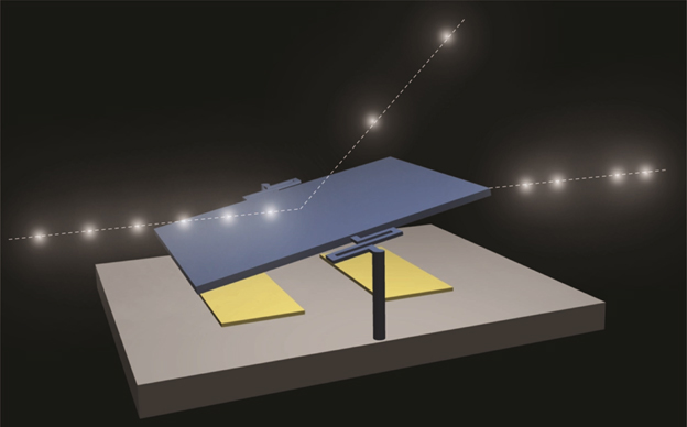
Scientists at Argonne's Center for Nanoscale Materials and APS have fabricated a torsional MEMS device made of silicon using a process similar to the manufacture of computer chips. Essentially, the device consists of a tiny diffracting silicon crystal suspended on opposite sides by a pair of torsional springs (see the figure). As the crystal tilts rapidly back and forth, it creates an optical filter that selects only the x-ray pulses desired for the experiment so that only x-rays diffracted at the Bragg angle from the crystal reach the sample under study. By adjusting the speed at which the MEMS device oscillates, researchers can control the timing of the x-ray pulses.
The device was successfully tested at the X-ray Science Division 7-ID-B,C,D undulator beamline at the APS, a beamline that is optimized for ultrafast experiments. The device was tested at 75 kHz, which allowed the team to pick individual pulses from a pulsed APS x-ray source with a very short temporal opening window of roughly three billionths of a second. This is about the closest pulse separation found at most of the synchrotron sources in the world. This device also can deliver x-ray pulses at 150 kHz, or 1 pulse in every 6 millionth of a second. It can be used for all hard x-ray wavelengths and one should be able to easily integrate it into a synchrotron radiation beamline at most of the light sources in the world. This demonstration of the successful application of the MEMS technology to manipulate or tailor an x-ray beam at very high frequencies will certainly lead to further more elaborate schemes using MEMS, and will enable advanced x-ray optical schemes for studying the structure and dynamics of matter at atomic length and time scales.
The versatility of the x-ray MEMS development based on the miniaturized optics can be further advanced to realize faster capabilities that will ultimately promise new ways to steer, filter, and shape x-ray pulses. An added bonus is that the MEMS fabrication technology allows flexibility in its operating specifications and allows their large scale production through scalability.As diffraction-limited x-ray storage rings come into operation, this device will be very useful; the new-generation sources will have densely-filled lattice and secondly, and the reduced beam profile requires even smaller scaled MEMS x-ray optics that can be more dynamic.
See: D. Mukhopadhyay, D.A. Walko, I.W. Jung, C.P. Schwartz, Jin Wang, D. López*, and G.K. Shenoy, “X-ray photonic microsystems for the manipulation of synchrotron light,” Nat. Commun. 6, 7057 (5 May 2015). DOI: 10.1038/ncomms8057
Author affiliation: Argonne National Laboratory
Correspondence: *[email protected]
This research used resources of the Advanced Photon Source and the Center for Nanoscale Materials, U.S. DOE Office of Science user facilities operated for the DOE Office of Science by Argonne National Laboratory under Contract No. DE-AC02-06CH11357.
Argonne National Laboratory is supported by the Office of Science of the U.S. Department of Energy. The Office of Science is the single largest supporter of basic research in the physical sciences in the United States, and is working to address some of the most pressing challenges of our time. For more information, please visit science.energy.gov.