
Purified silicon is a mainstay in today's sophisticated electronic devices, such as integrated circuits that are essential components of handheld computers, smart phones, and many every-day appliances. The semiconducting properties of the most common crystalline form of Silicon, the cubic diamond-structure (d-Si), has limitations that hinder it’s use in new types of devices. However, scientists from the Carnegie Institution for Science and the Muséum National d’Histoire Naturelle (France) have overcome this problem by synthesizing an entirely new form of silicon — an orthorhombic allotrope of silicon represented as Si24 — by utilizing a novel, two-step high-pressure thermal diffusion process. The researchers obtained important data about their new silicon by employing x-rays from the U.S. Department of Energy’s Advanced Photon Source, an Office of Science user facility, and at the European Synchrotron Radiation Facility (France). The potential exists for many exciting future applications of Si24 within the energy field. In fact, when used with more efficient precursor processes, Si24 could lead to dramatic enhancements in the efficiency of solar photovoltaic cells and LED based lighting.
Diamond-structured silicon (d-Si) is used in large amounts primarily because it is abundantly available (about 90% of the Earth's crust, 28% by mass, is composed of silicate minerals) and has relatively low production costs. It is also easily doped with other elements and possesses a native layer of passivating oxide. However, d-Si is only usable under certain conditions, such as when made very thick within solar cells so it can absorb sufficient amounts of light.
Further, in its commonly used form, d-Si (with a band gap of 1.1 eV) has indirect band gap semiconducting properties, rather than the more desired direct band gap. Generally, the band gap is the energy difference from the top of the valence band to the bottom of the conduction band, which ultimately determines the relationship between light absorption/emission and the flow of electrons. Having an indirect band gap means an extra step is required to excite bound electrons into a free state so they can participate in electrical conductivity. In other words, bound electrons cannot simply absorb or emit a photon when subjected to a specific amount of external energy; but, instead, require a phonon to initiate electronic excitations.
Thus, to overcome difficulties inherent in indirect bandgap semiconductors, these Carnegie scientists discovered a new polycrystalline compound of sodium and silicon, Na4Si24. This material was formed under high pressure (10 GPa, which equals 100,000 bar) and high temperature (at 1,070 K, or about 797° C).
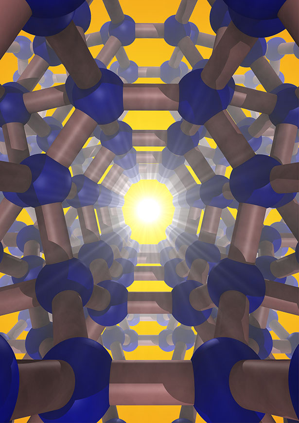
Then, this precursor compound was thermally "degassed" in a vacuum (approximately 10-5 T) at a temperature of 400 K, which slowly reduced its sodium content over an 8-day period. In what was a first-ever achievement, a pure, open framework structure comprised of channels with five-, six-, and eight-membered sp3-bonded silicon rings was synthesized. (Figure 1 indicates this open framework.) This is Si24.
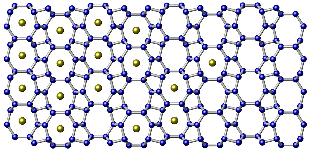
Energy-dispersive x-ray spectroscopy (EDXS) measurements showed that Si24 is at least 99.9% pure. (Figure 2 describes the ease in which sodium can diffuse through the lattice.) Si24 consists of a quasi-direct band gap of about 1.3 eV, an experimental value that agrees with these scientists' theoretical calculations and one that is highly sought after for use in photovoltaic applications.
Measurements were also taken before and after the completion of thermal degassing to determine sodium concentration. Angular dispersive powder x-ray diffraction data were collected at x-ray beamline 16-ID-B of the High Pressure Collaborative Access Team at the Argonne Advanced Photon Source, while monochromatic x-ray diffraction data were taken at beamline ID06 of the European Synchrotron Radiation Facility.
Both sets of experimental data showed the absence of sodium in the completely degassed samples, which is in agreement with theoretical conclusions.
The experimenters found that Si24 is stable up to a pressure of 10 GPa and a temperature of 750 K. They conclude that Si24 is a promising candidate, along with other previously undesirable materials, for wide applications from electrical energy storage to molecular-scale filtering.
Currently, the high-pressure precursor process, which is lengthy and expensive, limits the industrial applicability of Si24. However, these scientists believe that low-pressure methods, such as chemical vapor deposition, can eventually be developed to increase the production potential for Si24. When these limitations are solved, the potential for a new era of semiconductor technology could be realized.
— William A. Atkins
See: Duck Young Kim1, Stevce Stefanoski1, Oleksandr O. Kurakevych1,2, and Timothy A. Strobel1*, “Synthesis of an open-framework allotrope of silicon,” Nat. Mater. 14, 169 (February 2015). DOI: 10.1038/NMAT4140
Author affiliations: 1Carnegie Institution of Washington, 2Muséum National d’Histoire Naturelle
Correspondence: *[email protected]
The experimental work was supported by DARPA under contract numbers W31P4Q-13-1-0005 and W911NF-11-1-0300. The theoretical work was supported by Energy Frontier Research in Extreme Environments (EFree) Center, an Energy Frontier Research Center funded by the U.S. Department of Energy (DOE) Office of Science under award number DE-SC0001057. High Pressure Collaborative Access Team operations are supported by DOE-National Nuclear Security Administration under Award No. DE-NA0001974 and DOE-Basic Energy Sciences under Award No. DE-FG02-99ER45775, with partial instrumentation funding by the National Science Foundation. This research used resources of the Advanced Photon Source, a U.S. DOE Office of Science User Facility operated for the DOE Office of Science by Argonne National Laboratory under Contract No. DE-AC02-06CH11357.
Argonne National Laboratory is supported by the Office of Science of the U.S. Department of Energy. The Office of Science is the single largest supporter of basic research in the physical sciences in the United States, and is working to address some of the most pressing challenges of our time. For more information, please visit science.energy.gov.