
Many electronic devices — batteries, solar cells, transistors — work better under engineered strain. Carefully squeezing a semiconductor can improve its electron mobility so that current flows through it more easily, making the device more efficient. Modern computer chips depend on this effect, but the individual devices can be as small as tens of nanometers, so it’s important to understand exactly how strain can be applied at the smallest length scales.Previously, it had been difficult to study this without cutting the device open and altering the strain. Now, scientists have developed a new, non-destructive technique that lets them analyze spatial distortions inside the structure of a device using synchrotron x-rays from the U.S. Department of Energy’s Advanced Photon Source (APS), which could help them design even better devices.
The researchers from Argonne National Laboratory and IBM Research based their analysis on a technique, recently developed in the Argonne Materials Science Division, called Bragg projection ptychography (BPP), which creates structural maps from the diffraction patterns created when coherent x-rays are scattered off a structure. They made their measurements at the Hard X-ray Nanoprobe beamline 26-ID-C operated jointly by the Center for Nanoscale Materials (CNM) and the APS X-ray Science Division, which are Office of Science user facilities at Argonne. That beamline is one of the few worldwide that can focus hard x-rays to a 35-nanometer spot size with the ability to change beam position by less than 5 nanometers.
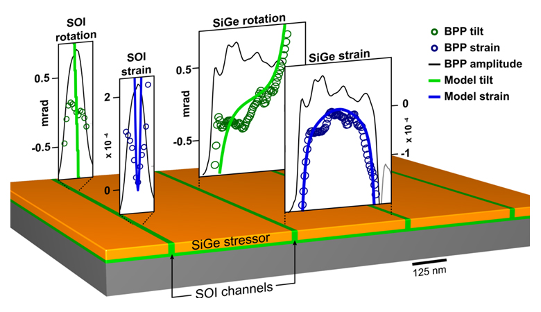
The team examined sample semiconductor devices provided by IBM Research that consisted of single-crystal silicon on a buried oxide insulator and etched into parallel channels 60 nanometers wide and 100 microns long, each separated by 460 nanometers. Silicon germanium was deposited between and on either side of those channels to impose stress on the silicon-on-insulator.
The researchers then scanned the x-ray beam over their device in a spiral pattern, recording coherent diffraction patterns and acquiring 16 spiral scans over 4 channel regions. Taking a spiral scan in overlapping steps of 13 nanometers gave them a resolution of ~10 nanometers, much smaller than the 30-nanometer spot size of the x-ray beam and enough to give them several points of reference across the 60-nanometer-wide silicon channel. X-rays scattering off the atomic lattice of the materials created interference patterns, which were caused both by changes in the orientation of the lattice and the sharp boundaries between the materials.
Mapping distortions in the atomic lattices revealed both lattice strain — the spacing of the atoms — and lattice tilt — the curvature of the structure (see the figure). This is the first time those two separate characteristics have been measured independently and quantitatively without sectioning, providing more detailed information than was previously available. The team compared their results to mechanical models of the nanostructure and found they were in good agreement.
This technique not only allows researchers to peer inside an intact structure, it can also be used to watch a device in operation, which can reveal how electronic behavior is related to mechanical properties of a structure. This ability could be useful for studying piezoelectric devices, which generate a current in response to mechanical stress or change shape in response to a current. It could also shed light on ferroelectric devices, which reverse their electrical polarization in response to an electric field.
A planned upgrade to the APS will allow researchers to use a more intense and even smaller x-ray spot at the CNM/APS Hard X-ray Nanoprobe, making their measurements more precise. The increased understanding from these studies may lead to more efficient nanoscale engineered materials such as transistors that operate on lower voltages, batteries less likely to produce excess heat, and more efficient photovoltaics. — Neil Savage
See: Martin V. Holt1*, Stephan O. Hruszkewycz1, Conal E. Murray2, Judson R. Holt2, Deborah M. Paskiewicz1, and Paul H. Fuoss1, “Strain Imaging of Nanoscale Semiconductor Heterostructures with X-Ray Bragg Projection Ptychography,” Phys. Rev. Lett. 112, 165502 (2014). DOI: 10.1103/PhysRevLett.112.165502
Author affiliations: 1Argonne National Laboratory, 2IBM
Correspondence: * [email protected]
This work, performed at the Center for Nanoscale Materials and use of the Advanced Photon Source, were both supported by the U. S. Department of Energy (DOE) Office of Science-Basic Energy Sciences, under Contract No. DE-AC02-06CH11357. S.O.H., D.M.P., and P.H.F. were supported by the U.S. DOE Office of Science-Basic Energy Sciences, Materials Sciences and Engineering Division.
Argonne National Laboratory is supported by the Office of Science of the U.S. Department of Energy. The Office of Science is the single largest supporter of basic research in the physical sciences in the United States, and is working to address some of the most pressing challenges of our time. For more information, please visit science.energy.gov.