
When thin films of ferroelectric materials are grown on single-crystal substrates, they can develop regions of aligned polarization — called "domains" — that often adopt complex patterns. Manipulation of ferroelectric domains can lead to advances in a number of technologies. However, in order to manipulate the domains, it is important to study their natural development. Previous studies have shown that interfacial strain and electrical boundary conditions play a large role. Accurate measurements of the local polarization can help science learn more. By changing the properties of the substrate and the interfaces of the ferroelectric materials, one can control the size and shape of the domains and thus influence the behavior of the material.
One promising method for doing so is called Bragg projection ptychography, or BPP. X-ray BPP had previously been used to measure strain in semiconductor devices. Now, a team of scientists from Argonne National Laboratory, the Korea Advanced Institute of Science and Technology, Northern Illinois University, and La Trobe University (Australia) carrying out studies at the U.S. Department of Energy Office of Science's Advanced Photon Source (APS) and Center for Nanoscale Materials at Argonne National Laboratory has found another application for BPP: imaging local polarization in ferroelectric thin films. In the future, this technique can help scientists study how domains develop in ferroelectric thin films, and thus how to manipulate them, potentially improving critical technologies such as memory storage.
First, the researchers used chemical vapor deposition to grow a 25-nm-thick film of the ferroelectric material lead titanate, or PbTiO3. When PbTiO3 is grown on a certain perfect single-crystal substrates, the domains will normally be distributed in a serpentine pattern. However, by controlling the surface properties of the substrate, these domain patterns can be influenced and controlled.
In this case, the researchers used substrates of strontium titanate, or SrTiO3, which had surface miscut steps spaced about 22-nm apart. Using a growth chamber at the Argonne Materials Science Division (MSD), they deposited PbTiO3 on the substrates, creating thin films with striped domain patterns.
That's where Bragg projection ptychography comes in. At the Center for Nanoscale Materials/X-ray Science Division beamline 26-ID-C, the researchers produced a focused coherent x-ray beam about 35-nm wide. When the beam hit the PbTiO3 film at a specific position and angle, it produced a coherent Bragg diffraction pattern — a sort of fingerprint of the local domain structure.
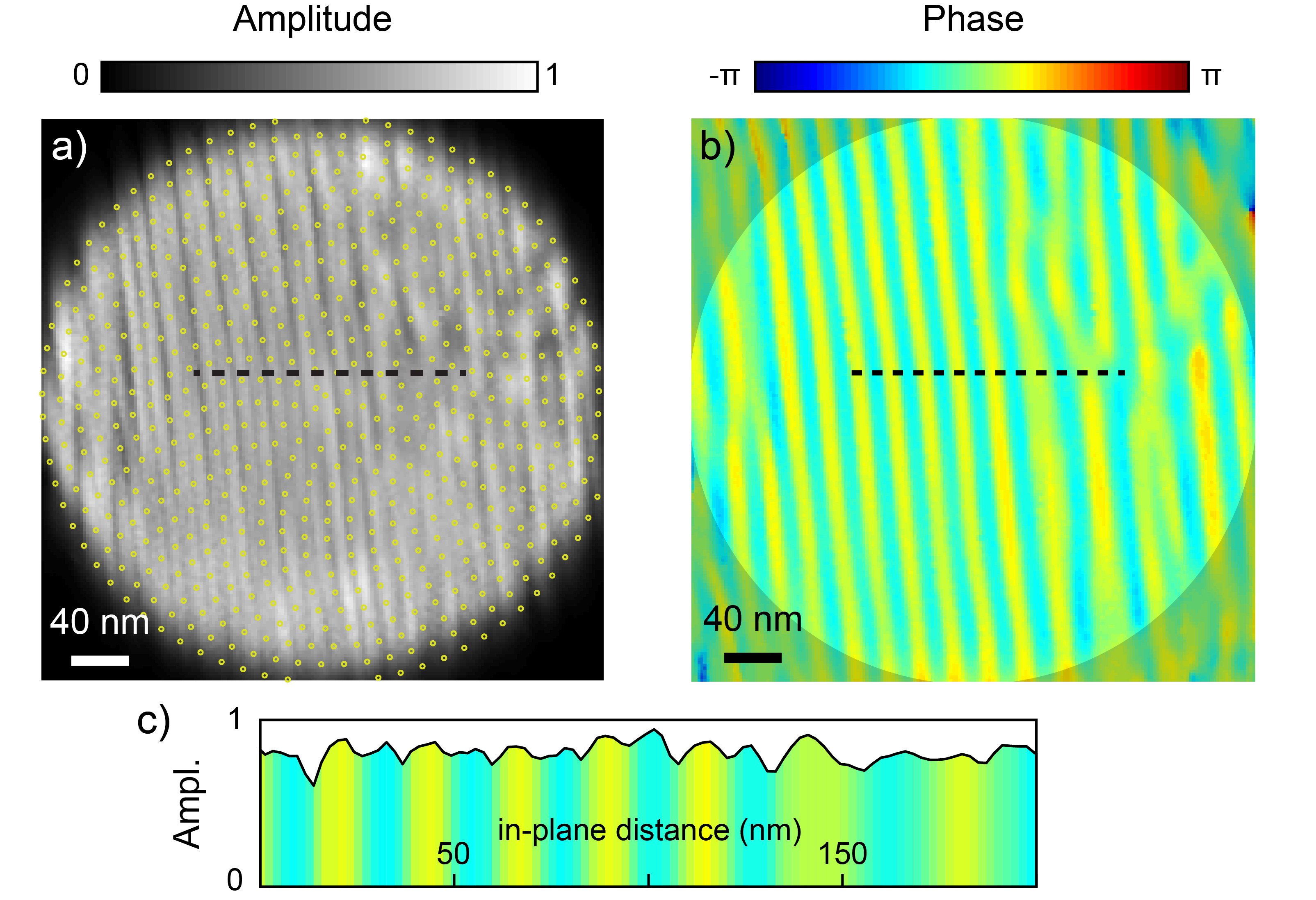
This process was repeated at about 650 points on the film, marked as yellow dots in part (a) of the figure. Because the x-ray beam was larger than the change in position, the information from all 650 points formed an overlapped data set.
Next, the team used a ptychographic algorithm, which simultaneously considered all the diffraction patterns from each overlapped point. With appropriate constraints, the algorithm converged to the correct answer in real space, converting the data from reciprocal space. Based on the resulting nanoscale map, the researchers created an image of the film's polarization, as shown in part (b) of the figure. The striped domain pattern they found was consistent with the structure of the PbTiO3 film's underlying SrTiO3 substrate.
To check the accuracy of the BPP reconstruction, the researchers also measured the local polarization of the PbTiO3 film with piezoresponse force microscopy. This method runs a scanning probe over the surface of the film to extract local polarization information.
Both techniques returned similar information about the domain pattern. However, piezoresponse force microscopy has a disadvantage: it requires direct access to the surface it is measuring. If a ferroelectric film was used as a memory device, it would be surrounded by layers of other electronic components, and this method of measuring polarization would be impossible.
BPP, on the other hand, can be performed from a distance, which means it can measure thin films in corrosive or enclosed environments where imaging with other techniques would be difficult or impossible. This makes BPP a promising tool for measuring how materials change under high temperatures and pressures.
— Sophie Bushwick
See: S.O. Hruszkewycz1*, M.J. Highland1, M.V. Holt1, Dongjin Kim1,2, C.M. Folkman1, Carol Thompson3, A. Tripathi4, G.B. Stephenson1, Seungbum Hong1,2, and P.H. Fuoss1, "Imaging Local Polarization in Ferroelectric Thin Films by Coherent X-Ray Bragg Projection Ptychography," Phys Rev. Lett. 110, 177601 (2013). DOI:10.1103/PhysRevLett.110.177601
Author affiliations: 1Argonne National Laboratory, 2Korea Advanced Institute of Science and Technology, 3Northern Illinois University, 4La Trobe University
Correspondence: *[email protected]
This work, including use of the Center for Nanoscale Materials and the Advanced Photon Source, was supported by the U.S. Department of Energy Office of Science, Basic Energy Sciences, under Contract No. DEAC02-06CH11357. S.O. H., M. J. H., D. K., C. M. F., S. H., and P. H. F. were supported by U.S. Department of Energy, Basic Energy Sciences, Materials Sciences and Engineering Division.
The Advanced Photon Source at Argonne National Laboratory is one of five national synchrotron radiation light sources supported by the U.S. Department of Energy's Office of Science to carry out applied and basic research to understand, predict, and ultimately control matter and energy at the electronic, atomic, and molecular levels, provide the foundations for new energy technologies, and support DOE missions in energy, environment, and national security. To learn more about the Office of Science x-ray user facilities, visit http://science.energy.gov/user-facilities/basic-energy-sciences/.
The Center for Nanoscale Materials at Argonne National Laboratory is one of the five DOE Nanoscale Science Research Centers (NSRCs), premier national user facilities for interdisciplinary research at the nanoscale, supported by the DOE Office of Science. Together the NSRCs comprise a suite of complementary facilities that provide researchers with state-of-the-art capabilities to fabricate, process, characterize and model nanoscale materials, and constitute the largest infrastructure investment of the National Nanotechnology Initiative. The NSRCs are located at DOE's Argonne, Brookhaven, Lawrence Berkeley, Oak Ridge and Sandia and Los Alamos National Laboratories.
Argonne National Laboratory seeks solutions to pressing national problems in science and technology. The nation's first national laboratory, Argonne conducts leading-edge basic and applied scientific research in virtually every scientific discipline. Argonne researchers work closely with researchers from hundreds of companies, universities, and federal, state and municipal agencies to help them solve their specific problems, advance America's scientific leadership and prepare the nation for a better future. With employees from more than 60 nations, Argonne is managed by UChicago Argonne, LLC for the U.S. Department of Energy's Office of Science.