
The reliability and longevity of electronics is critical to our interconnected world that is dependent upon internet and telecommunications technology. The computers, routers and switches, phones, and all the devices that link us together must be dependable down to the solder joints that connect integrated circuits to circuit boards, which can be an Achilles heel in an otherwise failure-free device.
Utilizing new synchrotron x-ray techniques and two synchrotron x-ray beamlines at the U.S. Department of Energy Office of Science’s Advanced Photon Source (APS), researchers from Cisco Systems, Inc.; Michigan State University; and the Max-Planck-Institut für Eisenforschung GmbH studied the beginnings of the thermal fatigue process in environmentally friendly, lead-free solder joints, as well as what happens toward the end of that process. These insights bring scientists a step closer to developing useful models for making physically based reliability predictions about solder-joint failure in this new material.
"With better understanding of how solder joint properties evolve, it will be possible extend the lifetimes of electronic systems" said Thomas Bieler of Michigan State University, a coauthor of the two Journal of Electronic Materials articles based on these studies.
The first century of electronics used lead-based solder because it has desired material properties for manufacturing and reliability. Engineers thoroughly understood the electrical, thermal, and structural behavior of these solders and were able to accurately predict reliability. In 2006, the European Union Restriction of Hazardous Substances Directive came into effect, banning lead-containing solders from all consumer electronics devices, manufacturers looked for alternative solder materials. But the ban created a new problem: How reliable were lead-free solders?
"Especially in the telecommunications industry, the expected lifetime of many products is long, and also a very low failure rate is needed," said coauthor Tae-Kyu Lee of the Component Quality and Technology Group at Cisco Systems.
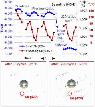
The researchers in this study developed new techniques and employed them at the APS to track the development of the failure mechanism of lead-free solder joints in situ for the first time. Working at the X-ray Science Division 6-ID-D and 34-ID-E beamlines at the Argonne National Laboratory APS, they conducted experiments to demonstrate how synchrotron x-ray diffraction could reveal the evolution of crystal orientation and strain patterns during thermal cycling in tin-containing, lead-free solder joints, specifically in the commonly used tin-silver-copper alloy SAC 305 (Sn-3%Ag-0.5% Cu).
Older lead-tin solders tend to solidify as a polycrystal, delivering a solder joint that has a uniform microstructure, with reproducible properties. But lead-free solders usually solidify either as a randomly oriented single crystal or a tricrystal. "With the lead-free solders, the properties of solder joints vary depending on both crystal orientation and position in the package, so it is important to identify worst-case scenarios to insure that lifetimes can be more accurately predicted" Bieler said.
Failures in lead-free solders don't always occur in areas where shear strains from thermal expansion mismatches are highest. This is a consequence of the non-cubic structure of tin and its highly anisotropic thermal expansion and stiffness. It is difficult to predict the strains that develop in an individual joint, given the random crystal orientation, so the prediction of damage is even more challenging. Furthermore, the crystal orientations evolve with thermal cycling. The experimenters examined SAC 305 joints both in a plastic ball grid array (PBGA) package sample and a wafer-level chip-scale package (WLCSP). Both types have been examined under thermal cycling, and the latter was studied in situ during melting, resolidification, and thermal cycling.
The advantages of the x-ray approach over the cross-sectional electron microscopy generally used to study solder joints were immediately apparent. "In a two-dimensional cross section, one does not necessarily know what has been removed or what is underneath the surface. With three-dimensional full illumination of the joint, we were able to prove that we did indeed primarily have single crystals in some joints and tricrystals in others," said Bieler.
"To clearly predict the lifetime of a certain joint,” said Lee, “we need to understand the failure mechanism. This study allowed us to see inside the joint while imposing thermal cycles in situ. Most of the earlier studies use destructive analysis to see the microstructure development after things happened. But the APS synchrotron lets us see the microstructure evolution during the event."
The x-ray diffraction measurements also provide a more dynamic picture of what happens inside the solder joint as it passes through different phases over time. For example, although there are only a few different tin crystal orientations in a given SAC lead-free solder joint, different orientations are always observed after melting and resolidification. Recrystallization behavior under thermal cycling also results in evolution of the tin crystal orientation.
Lee was excited about "the overall tin material response to the external factors. I considered tin as a 'dead' material with a certain crystal structure, but the more you look into this material, it seems to react like a living thing."
“What the APS data has especially enabled us to do is get a comprehensive picture of the very beginning of the thermal fatigue process [on beamline 6-ID-D] and connect it with what happens toward the end [on beamline 34-ID-E]," Bieler said.
Observing how the x-ray diffraction peaks changed from initial solidification and proceeded to spread out over repeated thermal cycles, Bieler said, "really helped us get to the point where we could describe the sequential mechanism from the moment of solidification up to the first crack that forms. We are able to explain everything that happened and why it happened in these solder joints as a result of what we've been able to do at the APS. The APS has been very helpful for understanding the early stage as well as the stage just before cracks form."
These fresh insights into the failure mechanism of lead-free solder joints guide scientists in their development of models for making reliability predictions. Although it is too early to proclaim any definite remedy for improving reliability in lead-free solder joints, the work provides some important clues.
"To find the right mitigation, you need to find the right failure mechanism," Lee said. "Based on the study so far, we identified that the grain refinement in tin interconnects reduce thermal cycling performance. But at the same time it is beneficial for resistance to mechanical shock. So there are no golden rules, but at least we are beginning to understand why."
As for next steps, Bieler said that "finding a reliable automated way to index diffraction patterns from multi-crystal joints would greatly speed up our ability to mine the data we have more effectively. Analysis strategies to obtain stress and strain would naturally follow using established methods. Continuing in situ measurements in thermomechanical cycling specimens, and looking toward comparing the microstructure before and after shock conditions (or possibly in situ), could also be effective. Microbeam diffraction in solder bumps is also a desirable thing to do, as the volumes are small, and this method is well suited for exploring tiny places." — Mark Wolverton
See: Bite Zhou1, Thomas R. Bieler1*, Guilin Wu2, Stefan Zaefferer2, Tae-Kyu Lee3, and Kuo-Chuan Liu3, “In Situ Synchrotron Characterization of Melting, Dissolution, and Resolidification in Lead-Free Solders,” J. Electron. Mater. 41(2), 262 (2012). DOI: 10.1007/s11664-011-1785-8
Author affiliations: 1Michigan State University; 2 Max-Planck-Institut für Eisenforschung
GmbH; 3Cisco Systems, Inc.
Correspondence: *[email protected]
And: Thomas R. Bieler1*, Bite Zhou1, Lauren Blair1, Amir Zamiri1, Payam Darbandi1, Farhang Pourboghrat1, Tae-Kyu Lee2, and Kuo-Chuan Liu2, “The Role of Elastic and Plastic Anisotropy of Sn in Recrystallization and Damage Evolution During Thermal Cycling in SAC305 Solder Joints,” J. Electron. Mater. 41(2), 283 (2012). DOI: 10.1007/s11664-011-1811-x
Author affiliations: 1Michigan State University; 2Cisco Systems, Inc.
Correspondence: *[email protected]
This research is supported by National Science Foundation-Grant Opportunities for Academic Liaison with Industry Contract 1006656; and Cisco Systems, Inc., San Jose, CA. Use of the Advanced Photon Source at Argonne National Laboratory was supported by the U.S. Department of Energy’s Office of Science under Contract No. DE-AC02-06CH11357. Most of the work was conducted by Ph.D. student Bite Zhou, and the support of beamline scientists Doug Robinson on beamline 6-ID-D and Wenjun Liu on beamline 34-ID-E enabled this success.
The Advanced Photon Source at Argonne National Laboratory is one of five national synchrotron radiation light sources supported by the U.S. Department of Energy’s Office of Science to carry out applied and basic research to understand, predict, and ultimately control matter and energy at the electronic, atomic, and molecular levels, provide the foundations for new energy technologies, and support DOE missions in energy, environment, and national security. To learn more about the Office of Science x-ray user facilities, visit http://science.energy.gov/user-facilities/basic-energy-sciences/.
Argonne National Laboratory seeks solutions to pressing national problems in science and technology. The nation's first national laboratory, Argonne conducts leading-edge basic and applied scientific research in virtually every scientific discipline. Argonne researchers work closely with researchers from hundreds of companies, universities, and federal, state and municipal agencies to help them solve their specific problems, advance America's scientific leadership and prepare the nation for a better future. With employees from more than 60 nations, Argonne is managed by UChicago Argonne, LLC for the U.S. Department of Energy's Office of Science.