
Like an ice cube on a warm day, most materials melt — that is, change from a solid to a liquid state — as they get warmer. But a few oddball materials do the reverse: They melt as they get cooler. Now a team of researchers from MIT, who utilized x-ray beamlines at two U.S. Department of Energy synchrotron x-ray light sources, including the Advanced Photon Source (APS) at Argonne National Laboratory, has found that silicon, the most widely used material for computer chips and solar cells, can exhibit this strange property of “retrograde melting” when it contains high concentrations of certain metals dissolved in it. Their findings could be useful in lowering the manufacturing cost of some silicon-based devices, especially those in which tiny amounts of impurities can significantly reduce performance.
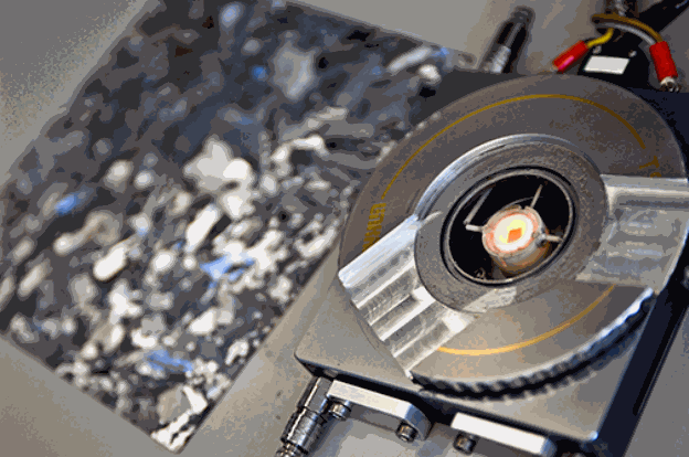
The material they studied, a compound of silicon, copper, nickel and iron, “melts” (actually turning from a solid to a slush-like mix of solid and liquid material) as it cools below 900 degrees Celsius, whereas silicon ordinarily melts at 1414 degrees C. The much lower temperatures made it possible to observe the behavior of the material during melting by employing x-ray fluorescence microprobe studies at the X-ray Operations and Research beamline 2-ID-D at the APS and the Advanced Light Source beamline 10.3.2 at the Lawrence Berkeley National Laboratory in California.
The material and its properties are described in a paper published in the journal Advanced Materials.
In the material that the researchers studied, impurities tend to migrate to the liquid portion, leaving regions of purer silicon behind. This could make it possible to produce some silicon-based devices, such as solar cells, using a less pure, and therefore less expensive, grade of silicon that would be purified during the manufacturing process.
“If you can create little liquid droplets inside a block of silicon, they serve like little vacuum cleaners to suck up impurities,” said Tonio Buonassisi of MIT and leader of the research team. This research could also lead to new methods for making arrays of silicon nanowires — tiny tubes that are highly conductive to heat and electricity.
Buonassisi predicted in a 2007 journal article that it should be possible to induce retrograde melting in silicon, but the conditions needed to produce such a state, and to study it at a microscopic level, are highly specialized and have only recently become available. To create the right conditions, Buonassisi and his team had to adapt a microscope “hot-stage” device that allowed the researchers to precisely control the rate of heating and cooling.
The material for the tests consisted of a kind of sandwich made from two thin layers of silicon, with a filling of copper, nickel, and iron between them. This was first heated enough to cause the metals to dissolve into the silicon, but below silicon’s melting point. The amount of metal was such that the silicon became supersaturated — that is, more of the metal was dissolved in the silicon than would normally be possible under stable conditions. For example, when a liquid is heated, it can dissolve more of another material, but then when cooled down it can become supersaturated, until the excess material precipitates out.
In this case, where the metals were dissolved into the solid silicon, “if you begin cooling it down, you hit a point where you induce precipitation, and it has no choice but to precipitate out in a liquid phase,” said Buonassisi. It is at that point that the material melts.
Correspondence: [email protected]
See: Steve Hudelson1, Bonna K. Newman1, Sarah Bernardis1, David P. Fenning1, Mariana I. Bertoni1, Matthew A. Marcus2, Sirine C. Fakra2, Barry Lai3, and Tonio Buonassisi1,*,“Retrograde Melting and Internal Liquid Gettering in Silicon,” Adv. Mater. 22(35), 3948 (September 15, 2010).
Author affiliations: 1Massachusetts Institute of Technology, 2Lawrence Berkeley National Laboratory, 3Argonne National Laboratory
Support for this research was provided by the U.S. Department of Energy, under contract number DE-FG36-09GO19001, and through the generous support of Doug Spreng and the Chesonis Family Foundation. S. Hudelson and D.P. Fenning acknowledge the National Science Foundation; B. Newman the Claire Boothe Luce Foundation. The Advanced Light Source and the Advanced Photon Source are supported by the Director, Office of Science, Office of Basic Energy Sciences, of the U.S. Department of Energy under Contracts No. DE-AC02-05CH11231 and DE-AC02-06CH11357, respectively.
The original MIT news release can be found at: http://news.mit.edu/press
The Advanced Photon Source at Argonne National Laboratory is one of five national synchrotron radiation light sources supported by the U.S. Department of Energy’s Office of Science, Office of Basic Energy Sciences (DOE-BES). The APS is the source of the Western Hemisphere’s brightest high-energy x-ray beams for research in virtually every scientific discipline. More than 3,500 scientists representing universities, industry, and academic institutions from every U.S. state and several foreign nations visit the APS each year to carry out applied and basic research in support of the BES mission to understand, predict, and ultimately control matter and energy at the electronic, atomic, and molecular levels in order to provide the foundations for new energy technologies and to support DOE missions in energy, environment, and national security. To learn more about the Office of Basic Energy Sciences and its x-ray user facilities, visit . Use of the APS was supported by the DOE-BES, under Contract No. DE-AC02-06CH11357.
Argonne National Laboratory seeks solutions to pressing national problems in science and technology. The nation's first national laboratory, Argonne conducts leading-edge basic and applied scientific research in virtually every scientific discipline. Argonne researchers work closely with researchers from hundreds of companies, universities, and federal, state and municipal agencies to help them solve their specific problems, advance America's scientific leadership and prepare the nation for a better future. With employees from more than 60 nations, Argonne is managed by UChicago Argonne, LLC for the U.S. Department of Energy's Office of Science.