
A new class of layered oxide materials discovered thanks to research at the U.S. Department of Energy’s Advanced Photon Source (APS) at Argonne National Laboratory offers scientists unprecedented opportunities for creating the next generation of electronic devices. These materials show intricate physical properties, resulting in a rich collection of phenomena including magnetic ordering, metal insulator transitions, superconductivity, magneto-resistivity, and ferroelectricity. Using these properties and the ability to tune them, scientists hope to create a new generation of all-oxide electronics that will enable new device functionalities not presently achievable.
A key challenge in creating this new class of electronics is finding materials that can operate above room temperature, and sorting out how subtle changes in their structure or composition influences their properties. Recently, scientists at Argonne, Ames Laboratory, the University of Illinois at Urbana Champaign, and Oak Ridge National Laboratory discovered such a phenomenon with research performed at the X-ray Operations and Research beamlines 6-ID and 33-BM at the APS.
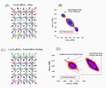
The work, recently published in Nature Materials, and led by scientists at Argonne, utilized grazing incidence x-ray diffraction to discover why thin films of La⅓Sr⅔MnO3, a well known antiferromagnet, could significantly the change magnetic ordering temperature. Typically, this system magnetically orders at 250K (TN), well below room temperature and therefore not readily functional in an electronic device. By designing the film in a superlattice analog the team managed to demonstrate magnetic order above room temperature.
Scientists at the Argonne’s Materials Science Division, Center for Nanoscale Materials, and the APS proposed a simple experiment: In the La⅓Sr⅔MnO3 (alloy) film both the lanthanum (La) and strontium (Sr) are randomly distributed. With very different atomic radii, one anticipates a local structural disturbance. If one were to separate the La and Sr into planes of their own, one expects disorder to be reduced and perhaps an increase in the TN. As anticipated, the ordering temperature indeed rose, by a significant 70K, the first time this compound would be magnetic above room temperature.
As is often the case in science, the measurement told a more fascinating story. The x-ray diffraction demonstrated that the random alloy film had an unexpected distortive structural periodicity, three unit cells long. The result was a strong local atomic distortion. However, in the superlattice, this periodicity was suppressed. This feature is likely a strain relief mechanism mitigating the tensile stress generated by forcing the film to larger lattice parameters imposed by the larger SrTiO3 substrate. What, then, mitigates the strain in the superlattice film? What occurs is the unprecedented emergence of an ultra-long distortive order, a 60-unit-cell super-periodicity. The dramatic rise of the magnetic ordering temperature was simply due to the reduction of local disorder as the atoms oscillated over much longer length scales. In reality, the superlattice film is more than just a simple analog, it is a new material with its own inherent characteristics.
Fundamentally, atoms will always seek the place of lowest energy. As we confine, engineer, and chemically select the atoms where and how we would like them, the system will collectively respond to find new local minima. The task is to discover and understand the nature of such local minimum energy states and learn how they may enhance or perhaps hinder the application of these new exciting materials.
— Philip Ryan
See: S.J. May1, P.J. Ryan2*, J.L. Robertson3, J.-W. Kim1, T.S. Santos1, E. Karapetrova1, J.L. Zarestky4, X. Zhai5, S.G.E. te Velthuis1, J.N. Eckstein5, S.D. Bader1, and A. Bhattacharya1**, “Enhanced ordering temperatures in antiferromagnetic manganite superlattices,” Nat. Mater. 8, 892 (November 2009). DOI:10.1038/NMAT2557
Author affiliations: 1Argonne National Laboratory, 2Ames Laboratory, 3Oak Ridge National Laboratory, 4Ames Laboratory and Iowa State University, 5University of Illinois at Urbana-Champaign
Correspondence: *[email protected], ** [email protected]
Work at Argonne, including use of the Advanced Photon Source and the Center for Nanoscale Materials, was supported by the U.S. Department of Energy, Office of Science, Office of Basic Energy Sciences, under contract No DE-AC02-06CH11357. Work at Oak Ridge National Laboratory's High Flux Isotope Reactor was sponsored by the Scientific User Facilities Division, Office of Basic Energy Sciences, U.S. Department of Energy.