
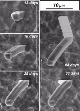
A short circuit can be quite hairy. Satellites have failed, a NASA computer center was repeatedly paralyzed, and the U.S. public health authority recalled thousands of pacemakers—all because tin whiskers caused a short circuit in the electronic components of these devices. Tin whiskers can be up to a few millimeters long and just a few micrometers in diameter. They sprout from the tin used to solder and plate electronic components made of copper. Understanding in detail what makes the whiskers grow is the first step on the way to preventing their growth. A team of scientists used the U.S. Department of Energy’s Advanced Photon Source (APS) at Argonne in their research aimed at measuring the forces that trigger this metallic hair growth. Their results were published in Applied Physics Letters.
The NASA computer center system failures began after new data storage had been installed. At least 18 short circuits occurred in the high-performance computers before technicians found the reason: The replacement of the storage devices dislodged metal whiskers from the base construction, and their subsequent distribution via air circulation caused system failure by bridging the electrical circuits of the supercomputers.
Researchers from the Robert Bosch GmbH, Argonne, and Oak Ridge National Laboratory working with Eric J. Mittemeijer, Director of the Max Planck Institute for Metals Research, have revealed the forces that cause these whiskers to sprout from tin-plated copper. According to their findings, the pressure of the tin atoms at the base of the film needs to be higher than at the surface. At the same time, there must be a pressure difference on the film’s surface plane: The pressure at the root of the tin whisker must be lower than it is further away. “You can compare it to a toothpaste tube,” said Matthias Sobiech, who carried out the experiments. “When you press the sides, toothpaste comes out of the top.” The pressure, which physicists also call stress, is created because an intermetallic tin-copper compound forms at the tin-copper interface that grows further into the tin film.
X-ray investigations carried out at both laboratory and synchrotron (the X-ray Operations and Research 34-ID-E x-ray beamline at the APS) provided a detailed picture of the distribution of the stress in the tin film. The researchers determined the stress differences between the base and the surface of the tin film in their laboratory in Stuttgart by measuring, step-by-step, the vertical mechanical stresses. In order to measure the distribution of stress in the surface plane around a growing whisker, the researchers had to use a method with very high spatial resolution in the sub-micron range. These micro-stress measurements were taken using the micro Laue diffraction technique: A very fine beam of x-rays, around 300 nanometers in diameter, scanned the surroundings of a growing tin whisker in very small steps, and a sensitive detector very precisely recorded the local stresses at each probed position.
“We showed, for the first time, that tin whiskers are formed on tin layers, which clearly exhibit mechanical stress differences,” said Mittemeijer, “and that these stress differences are the driving force for the growth of the whiskers.” He and his colleagues demonstrated this in experiments by measuring local stress distributions in films that exhibit whisker growth and in films that do not exhibit whisker growth.
Looking closely at the state of stress in a material can be helpful in many investigations. It reveals a lot about the forces that operate in electronic or mechanical microsystems, which might have a detrimental effect on their function in the same way the tin whiskers cause short circuits in electronic components. “We hope that our findings will help to protect electronic components from the growth of tin whiskers,” said Sobiech, “because we now know that it is important to remove the stress differences in the film.” The researchers are setting out to investigate how that can be done.
See: M. Sobiech1,2, M. Wohlschlögel1, U. Welzel1, E.J. Mittemeijer1*, W. Hügel2, A. Seekamp2, W. Liu3, and G.E. Ice4, “Local, submicron, strain gradients as the cause of Sn whisker growth,” Appl. Phys. Lett. 94, 221901 (2009). DOI: 10.1063/1.3147864
Author affiliations: 1Max Planck Institute for Metals Research, 2Robert Bosch GmbH, 3Argonne National Laboratory, 4Oak Ridge National Laboratory
Correspondence: *[email protected]
The authors are much obliged to the company Hans Heimerdinger Oberflächentechnik in Pforzheim, Germany, for specimen preparation. Use of the Advanced Photon Source was supported by the U.S. Department of Energy, Office of Science, Office of Basic Energy Sciences (DOE-BES) under Contract No. DEAC02-06CH11357. G.E.I. was supported by the Division of Material Sciences and Engineering, DOE-BES.
The original Max Planck Society news release can be found here.
Use of the Advanced Photon Source is supported by the U.S. Department of Energy, Office of Science, Office of Basic Energy Sciences, under Contract No. DE-AC02-06CH11357.
Argonne National Laboratory seeks solutions to pressing national problems in science and technology. The nation's first national laboratory, Argonne conducts leading-edge basic and applied scientific research in virtually every scientific discipline. Argonne researchers work closely with researchers from hundreds of companies, universities, and federal, state and municipal agencies to help them solve their specific problems, advance America's scientific leadership and prepare the nation for a better future. With employees from more than 60 nations, Argonne is managed by UChicago Argonne, LLC for the U.S. Department of Energy's Office of Science.