
Pile-ups, bad enough on the freeway, also are a hazard for the makers of high-performance strained-silicon (Si) semiconductor devices. A sensitive x-ray diffraction imaging technique developed by researchers at the National Institute of Standards and Technology (NIST) can help manufacturers avoid the latter—a bunching up of crystal defects caused by the manufacturing process for strained-silicon films.
Strained silicon is a new, rapidly developing material for building enhanced-performance silicon-based transistors. Introducing a slight tensile strain in the lattice of the silicon crystal dramatically improves the mobility of charges in the crystal, enabling faster, higher-performance devices. The strain is achieved by first growing a relatively thick crystalline layer of silicon-germanium (SiGe) on the normal silicon substrate wafer, and then growing a thin film of pure silicon on top. The difference in lattice spacing between pure silicon and SiGe creates the desired strain, but also creates occasional defects in the crystal that degrade performance. The problem is particularly bad when the defects cluster together in so-called “pile-ups.”
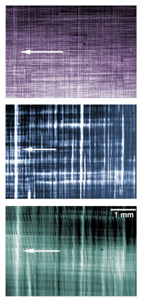
One of the best methods for studying crystal defects is to observe the image of x-rays diffracted from the crystal planes, a technique called x-ray topography. Until now, however, it’s been impossible to study the interaction of defects in the multiple layers of these complex Si-SiGe-Si wafers. In a recent paper in Applied Physics Letters, researchers from NIST and AmberWave Systems Corporation (Salem, N.H.) detail a high-resolution form of x-ray topography that can distinguish individual crystal defects layer by layer. The technique combines an extremely low-angle incident x-ray beam (“glancing incidence”) to increase the signal from one layer over another and the use of highly monochromatic x-rays tuned to separate the contributions from each layer based on their different lattice spacings.
Their results show that crystal defects initially created at the interface between the silicon wafer and the SiGe layer become “templates” that propagate through that layer and create matching defects in the strained-silicon top layer. These defects, in turn, are notably persistent, remaining in the strained-silicon even through later processing that includes stripping the layer off, bonding it to an oxidized silicon wafer, and annealing it to create strained-silicon-on-insulator substrates.
See: D.R. Black, J.C. Woicik, M. Erdtmann and T.A. Langdo, “Imaging defects in strained-silicon thin films by glancing-incidence x-ray topography,” Appl. Phys. Lett. 88, 224102. (2006). DOI: 10.1063/1.2209411
The complete NIST article (3rd story on page) is at https://www.nist.gov/public_affairs/techbeat/tb2006_0706.htm
The research was performed at the X-ray Operations and Research beamline 33-BM at the U.S. Department of Energy’s (DOE’s) Advanced Photon Source at Argonne National Laboratory and supported in part by the DOE. Use of the Advanced Photon Source was supported by the U.S. Dept. of Energy, Office of Science, Basic Energy Sciences, under Contract No. W-31-109-ENG-38.
Argonne National Laboratory is a U.S. Department of Energy laboratory managed by The University of Chicago