Ultrathin films of electronic materials have been shown to exhibit remarkable physical properties. Some of these ultrathin films, known as monolayers, are only a single molecular layer thick. While such exceedingly thin films can be formed from a variety of layered compounds, it has proven difficult to coax organic polymers to reliably form highly-ordered, ultrathin sheets. Scientists would like to develop such polymer films because they consist of inexpensive and environmentally-friendly ingredients, are flexible, and their properties depend on their ordering, making them tunable. A team of researchers has now demonstrated a simple printing process that consistently yields high-quality ultrathin polymer films, with thicknesses ranging from several molecular layers down to monolayers, or about one ten-thousandth the diameter of a human hair. Controlling film thickness allowed the team to vary the film's properties. Moreover, the researchers successfully printed ultrathin films from different polymers, and transferred them to different substrates. The polymer chains in the ultrathin films were characterized using high-brightness x-rays at the U.S. Department of Energy’s Advanced Photon Source (APS). The relatively simple techniques demonstrated by the researchers and published in the journal Advanced Functional Materials may lead to the mass production of inexpensive, ultrathin polymer films down to monolayer thickness, with potential applications including photovoltaics, sensors, and wearable electronics.
Plastic consists of polymers, long chain molecules made up of many smaller, identical molecular units. Conjugated polymers, which played a key role in this study, are organic (carbon-based) polymers featuring a long molecular backbone with alternating single and double chemical bonds, a structure that allows these polymers to conduct charge, unlike most plastic materials, which are insulating. Conjugated polymers are known as organic (carbon-based) semiconductors (OSCs) because they have properties similar to silicon, and can also form the basis for transistors and other electronic devices. Previous studies have demonstrated the considerable potential of monolayer films of conjugated polymers, with unique optoelectronic and outstanding sensing properties. In spite of this considerable potential, efforts to develop a reliable and cost-effective technique for producing such monolayers have proven elusive. For instance, some fabrication methods yield monolayers composed of networks of one-dimensional polymer fibers instead of a truly uniform, two-dimensional (2-D) film.
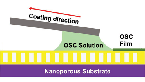
The scientists conducting this study, from the University of Illinois at Urbana-Champaign, overcame these shortcomings and produced highly-ordered 2-D monolayers of conjugated polymers on various substrates. The first challenge involved selecting a method to rapidly lay down polymers over a large area. The team developed the meniscus-guided coating (MGC) method, which facilitates controlled deposition of polymers and provides directionality for their ordering. The MGC technique is illustrated in Fig. 1. A liquid infused with conjugated polymers is sandwiched between a substrate and a coating blade. The liquid adheres to both surfaces, which are placed fractions of a millimeter apart. As the coating blade moves it drags the liquid over the substrate. As the film dries it leaves behind a sheet of conjugated polymers. Changing the blade's speed, its distance from the substrate, and the concentration of the solution varied the film's thickness, which in turn changed its structure and properties.
The other key technology is dynamic-template. It involves infusing a special ionic liquid (IL) into a substrate riddled with nanoscale voids (bottom of Fig. 1). The strong interaction between the polymer and the IL, along with the dynamic nature of the liquid surface, helped crystallize highly-ordered 2-D monolayer films. Another advantage of dynamic-template is the wide range of substrates that can be used for film transfer, including rigid and flexible materials.
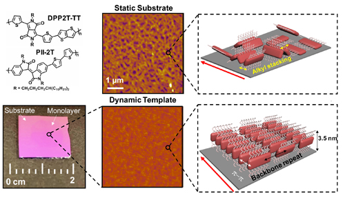
Several ultrathin films were produced using two different conjugated polymers, abbreviated DPP2T-TT and PII-2T. Combining the dynamic-template and MGC techniques, the researchers created ultrathin films with varying thicknesses. These films were later transferred from the nanoporous substrate to both rigid and flexible substrates, thus illustrating the utility of the new approach. For comparison purposes, an ultrathin film formed on a static substrate did not incorporate an ionic liquid or nanoporous substrate. The structures of all the ultrathin films were characterized by grazing incidence x-ray diffraction at APS beamline 8-ID-E, which is operated by the X-ray Science Division Dynamics & Structure Group. The sensitivity of the technique is sufficient to detect crystallinity in even the thinnest films studied, and the versatility of the sample environment allowed the scientists to observe how the structure differed parallel and perpendicular to the MGC printing direction.

Figure 2 compares a monolayer film deposited on a static substrate with a monolayer film produced using the dynamic-template-assisted MGC approach. The static substrate film (upper half of Fig. 2) is riddled with voids that lead to poor conduction. By contrast, the dynamic-template film (lower half) appears smooth with a highly-ordered polymer structure and enhanced charge transport properties.
These research results provide new insights into the morphological, electronic, and sensing performance of ultrathin conjugated polymer films, especially how these properties vary with thickness. A practical spin-off was also demonstrated. A 7-nanometer-thick film showed an ultrahigh sensitivity to gaseous ammonia, at a concentration of only one part per billion. The researchers speculate that such ultrathin films could serve as inexpensive, disposable ammonia detectors for spotting the early stages of kidney failure, when ammonia occurs in patients’ breath. ― Philip Koth
See: Prapti Kafle, Fengjiao Zhang, Noah B. Schorr, Kai-Yu Huang, Joaquín Rodríguez-López, and Ying Diao*, “Printing 2D Conjugated Polymer Monolayers and Their Distinct Electronic Properties,” Adv. Funct. Mater. 30, 1909787 (2020). DOI: 10.1002/adfm.201909787
Author affiliation: University of Illinois at Urbana-Champaign
Correspondence: *yingdiao@illinois.edu
This research was primarily supported by the National Science Foundation (NSF) Materials Research Science and Engineering Centers: Illinois Materials Research Center under grant number DMR 17-20633. P.K. acknowledges partial support from American Association of University Women (AAUW) International fellowship. Y.D. and K.-Y. H. were partially supported by NSF CAREER award under grant number NSF DMR 18-47828. Y.D. acknowledges partial support from the JITRI International Fellowship. The authors are grateful to beamline scientist Joseph Strzalka of the APS for facilitating the grazing incidence x-ray diffraction measurements. This research used the resources of the Advanced Photon Source, a U.S. DOE Office of Science User Facility operated for the DOE Office of Science by the Argonne National Laboratory under contract no. DE-AC02-06CH11357.
The U.S. Department of Energy's APS is one of the world’s most productive x-ray light source facilities. Each year, the APS provides high-brightness x-ray beams to a diverse community of more than 5,000 researchers in materials science, chemistry, condensed matter physics, the life and environmental sciences, and applied research. Researchers using the APS produce over 2,000 publications each year detailing impactful discoveries, and solve more vital biological protein structures than users of any other x-ray light source research facility. APS x-rays are ideally suited for explorations of materials and biological structures; elemental distribution; chemical, magnetic, electronic states; and a wide range of technologically important engineering systems from batteries to fuel injector sprays, all of which are the foundations of our nation’s economic, technological, and physical well-being.
Argonne National Laboratory seeks solutions to pressing national problems in science and technology. The nation's first national laboratory, Argonne conducts leading-edge basic and applied scientific research in virtually every scientific discipline. Argonne researchers work closely with researchers from hundreds of companies, universities, and federal, state and municipal agencies to help them solve their specific problems, advance America's scientific leadership and prepare the nation for a better future. With employees from more than 60 nations, Argonne is managed by UChicago Argonne, LLC, for the U.S. DOE Office of Science.
The U.S. Department of Energy's Office of Science is the single largest supporter of basic research in the physical sciences in the United States and is working to address some of the most pressing challenges of our time. For more information, visit the Office of Science website.
